PCB Design Services | Professional PCB Layout & Design - KKPCB
 
HomeCategory

PCB Design Services | Professional PCB Layout & Design - KKPCB

Overview of Copper Foil for PCB Laminates

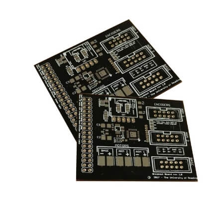
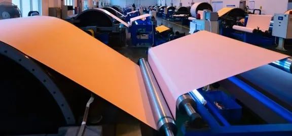
Copper foil used in the PCB industry is more complex than you might think. Copper is both an excellent conductor of electricity and an excellent conductor of heat, making it an ideal conductor for most PCB applications. Copper foil has many other properties that are important for engineers to understand. The copper foil used in the PCB...

EMI Solution in Multilayer PCB Design

There are many ways to solve the EMI problem. Modern EMI suppression methods include: using EMI suppression coatings, selecting appropriate EMI suppression components and EMI simulation design, etc. This article starts with the most basic PCB layout and discusses the role and design techniques of PCB layer stacking in controlling EMI radiation. Power Bus Placing...

Printed Circuit Board Basics: From Design to Final Artwork

Key Takeaways Defining two major concepts of PCB board design and production: class and build. An overview of the PCB layout department’s responsibilities: library part generation as well as placement and routing. Stepping more granularly through each task from schematic/design document reception to manufacturing files. Electronic devices saturate the modern world. Whether it is a...

Maximize Performance With PCB Cross-Hatching

Key Takeaways Cross-hatching significantly increases the flexibility of flex PCBs by reducing copper content. Helps maintain optimal impedance in flex PCBs without altering dielectric thickness or signal line width. Enables efficient manufacturing with reduced copper usage and improved resin adhesion. Cross-hatch PCB connector PCB cross-hatching is a technique where certain planes or large copper areas are designed...

Rigid Flex PCB Cost Optimization

Master Your Budget: Proven Strategies for Rigid Flex PCB Cost Optimization In modern electronics, Rigid-Flex PCB technology is the gold standard for compact, high-reliability designs. However, the complexity of Rigid-Flex manufacturing often leads to higher production expenses. Achieving effective Rigid Flex PCB cost optimization requires a strategic balance between sophisticated engineering and smart logistical choices. At KKPCB, we help engineers navigate these...

How to Check for PCB Warpage: Techniques and Methods

Key Takeaways Stress during fabrication, such as thermal expansion and contraction, imbalanced copper distribution, and improper handling, can lead to warpage. Utilize tools like feeler gauges, height gauges, contour gauges, optical profilometers, and Finite Element Method (FEM) simulations to accurately measure PCB warpage. Effective design practices using OrCAD X, such as symmetrical component placement and...

How to Create a Variable Power Supply PCB Layout

A variable power supply PCB is one of the most essential designs in electronic engineering, lab equipment, industrial systems, and embedded development platforms. It allows adjustable output voltage and current, making it suitable for testing, prototyping, and powering sensitive circuits. Designing a reliable variable power supply PCB layout requires careful consideration of power integrity, thermal...

Prototype PCB Design Software Essentials

Key Takeaways The competitiveness of new product introduction makes it critical to optimize your prototype design process for effectiveness and efficiency. Your prototype PCB design software should exhibit essential attributes for managing component inventory, creating schematics, designing PCBs, verifying designs, and managing data. OrCAD X delivers the essential functionality and capabilities in one program for prototype design...

Introduction to PCB Design

PCB design involves two critical stages: component layout and circuit connection wiring. The layout is the arrangement of circuit components within the PCB’s wiring area. A well-thought-out layout directly affects the ease of subsequent wiring and significantly impacts the PCB’s overall performance. In addition to meeting circuit functionality and performance requirements, a good layout considers manufacturability, inspection, and maintenance....

Electromagnetic Compatibility Design of Mobile Phone PCB

Electromagnetic compatibility (EMC) refers to the ability of electronic devices to function harmoniously in their electromagnetic environment without causing or being affected by electromagnetic interference (EMI). The goal of EMC design is to enable electronic devices to resist external interference while minimizing the electromagnetic interference they emit to surrounding devices. 1. Selecting the Right Wire Width Minimizing inductance...