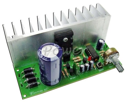
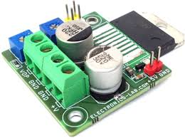
A variable power supply PCB is one of the most essential designs in electronic engineering, lab equipment, industrial systems, and embedded development platforms. It allows adjustable output voltage and current, making it suitable for testing, prototyping, and powering sensitive circuits.
Designing a reliable variable power supply PCB layout requires careful consideration of power integrity, thermal management, noise suppression, and component placement. Poor layout can lead to voltage instability, overheating, and excessive ripple noise.
This guide explains how to design an efficient and stable variable power supply PCB layout step by step.
Understanding Variable Power Supply Architecture
A typical variable power supply PCB consists of the following blocks:
1. Input Stage
- AC input (via transformer or SMPS input)
- Rectifier bridge (AC to DC conversion)
- Input filtering capacitors
2. Voltage Regulation Stage
- Linear regulator (e.g., LM317) or switching regulator (buck converter)
- Feedback network for voltage adjustment
- Reference voltage circuit
3. Output Stage
- Adjustable output terminals
- Current limiting circuit (optional but recommended)
- Output filtering capacitors
4. Protection Circuit
- Overcurrent protection
- Overvoltage protection
- Thermal shutdown (if supported by regulator IC)
Key Design Goals for PCB Layout
When designing a variable power supply PCB, the main objectives are:
- Stable and noise-free output voltage
- Efficient heat dissipation
- Low ripple and EMI
- High current handling capability
- Safe operation under load variations
PCB Layout Best Practices
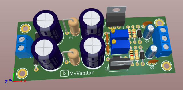
1. Component Placement Strategy
Proper placement is the foundation of a good power supply PCB layout:
- Place input rectifier and filter capacitors close together
- Keep regulator IC near heat sink or board edge
- Place output capacitors as close as possible to load output pins
- Separate high current and low signal paths
Poor placement leads to voltage drop and noise coupling.
2. Power Trace Design
Power traces carry high current and must be carefully designed:
- Use wide copper traces for power paths
- Increase copper thickness (2 oz recommended for high current designs)
- Avoid sharp corners in high-current routing
- Use copper pours for VCC and GND planes
Current density must be minimized to avoid overheating:
J=IAJ = \frac{I}{A}J=AI
3. Grounding Strategy (Very Important)
Good grounding ensures stable voltage output and low noise:
- Use star grounding topology
- Separate power ground and signal ground
- Connect all grounds at a single point near input capacitor
- Avoid ground loops
4. Thermal Management Design
Variable power supplies often dissipate significant heat:
- Place regulator IC near PCB edge for airflow
- Use thermal vias under regulator pad
- Add large copper area for heat spreading
- Consider external heat sinks for high current designs
Power dissipation must be controlled:
P=(Vin−Vout)⋅IP = (V_{in} – V_{out}) \cdot IP=(Vin−Vout)⋅I
5. Noise and Ripple Reduction
To ensure clean DC output:
- Use low ESR capacitors
- Add LC filters at output stage
- Keep switching loops short (for SMPS designs)
- Separate analog feedback traces from power traces
6. Voltage Adjustment Circuit Layout
For adjustable regulators (e.g., LM317):
- Keep feedback loop short and direct
- Avoid routing near high-current traces
- Use precision resistors for stable output
- Add bypass capacitor near adjust pin
7. High Current Design Considerations
For high current variable power supplies:
- Use parallel copper pours
- Reinforce vias for current transfer
- Increase PCB thickness if needed
- Use multiple layers for power distribution
8. EMI Control Techniques
Especially important for switching power supplies:
- Minimize loop area in switching paths
- Use ground shielding under switching nodes
- Add ferrite beads on input/output lines
- Keep high dv/dt nodes away from feedback circuits
Common Mistakes to Avoid
- Thin power traces causing overheating
- Poor grounding leading to unstable output
- Long feedback loops causing oscillation
- Insufficient decoupling capacitors
- Ignoring thermal design
Applications of Variable Power Supply PCBs
- Electronics lab bench supplies
- Industrial test systems
- Battery charging systems
- Embedded system development
- LED driver testing
- Prototyping platforms
Conclusion
Designing a variable power supply PCB layout requires a balance between power integrity, thermal management, and noise control. By optimizing trace width, grounding strategy, component placement, and heat dissipation, engineers can achieve stable and efficient power regulation.
A well-designed layout ensures low ripple output, high efficiency, and long-term reliability, making it suitable for both lab and industrial applications.
