kkpcba-Cindy - KKPCB - Page 46 of 75
 
HomeAuthor

kkpcba-Cindy - KKPCB - Page 46 of 75

Guide to Restoring Circuit Diagrams from Physical PCBs

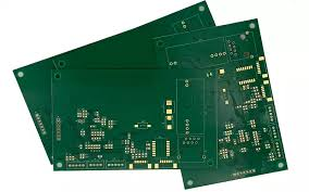
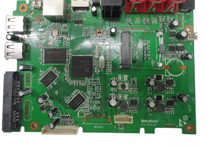
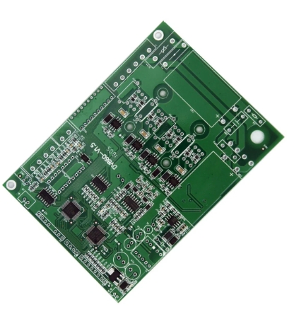
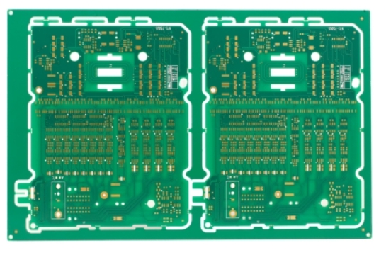
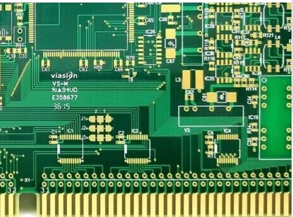
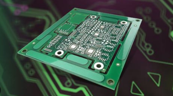
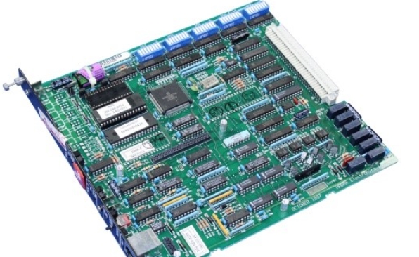
Often, products come without a circuit schematic, making it challenging to understand the PCB’s functionality and design principles. When faced with such a situation, follow these steps to reverse-engineer and restore the circuit diagram. This guide provides detailed instructions for accurately translating a physical PCB back into a schematic diagram. Steps to Restore a Circuit...

Common Problems and Solutions for Substrates in PCB Design

In modern PCB design, the choice and handling of substrate materials play a critical role in determining the overall performance, reliability, and manufacturability of the circuit board. Substrate-related issues can lead to serious defects such as poor solderability, delamination, signal loss, and even complete product failure. This article outlines the most common substrate problems encountered...

PCB Interconnection Methods

The interconnection of electrical contacts between components and electromechanical parts in a PCB ensures the system functions as per the circuit schematic. Selecting an appropriate interconnection method depends on the specific application, balancing reliability, processability, and cost. Below are commonly used PCB interconnection methods, along with their advantages, considerations, and application scenarios. 1. Soldering Method This...

PCB Manufacturing Packaging Process

Proper packaging plays a crucial role in ensuring the safe delivery of PCBs, particularly in competitive markets where quality and presentation are key factors. Though packaging may not generate direct added value, it impacts customer satisfaction and reflects professionalism, particularly for high-precision products like PCBs. This article discusses the importance of packaging, the evolution of...

5 Key Points in PCB Design for Power Supply Applications

In power supply design, PCB layout plays a critical role in ensuring the circuit’s efficiency, stability, and reliability. Below are five essential considerations for effective PCB design in power supply applications: 1. Establish a Logical and Linear Signal Flow Directionality is crucial in PCB design to minimize interference and ensure smooth operation. Segregation of Signals: Separate input/output, AC/DC, strong/weak signals,...

Essentials of PCB Design: Grounding Considerations

Grounding is a critical aspect of PCB design, particularly in mixed-signal environments where digital and analog circuits coexist. Proper grounding ensures stable performance, minimizes noise, and improves the reliability of the overall circuit. Below are key insights and guidelines to address grounding challenges effectively. Key Grounding Concepts Analog Ground (AGND) vs. Digital Ground (DGND): Purpose: Separate analog...

Factors Affecting the Quality of PCB SMT Laser Steel Mesh

1. Manufacturing Process The best manufacturing process includes electropolishing after laser cutting. Processes like chemical etching and electroforming are prone to errors, such as issues in film making, exposure, or substrate unevenness. 2. Materials Used Steel Mesh Frame: Must withstand a degree of pressure and maintain levelness. Screen: Polyester mesh is ideal for long-term stable tension. Steel Sheet: Type 304 matte finish is preferred...

Classification and Parameters of PCB Board Materials: Comprehensive Guide

Overview of PCB Materials Printed Circuit Boards (PCBs) are fabricated using various materials to meet specific performance and application requirements. In China, PCB copper-clad laminates (CCLs) are extensively used, and they can be categorized by base materials, resin adhesives, flame retardancy, and performance levels. Types of Copper-Clad Laminates (CCLs) 1. Classification by Reinforcement Material Paper-based materials: Typically used for low-cost...

High-Speed PCB Design Guide XI: How to Improve Testability

As electronic devices become increasingly miniaturized, advancements in component and wiring technologies have created new challenges for production testing. Highly integrated ICs, smaller insulation spacings, and limited access to circuit nodes have made traditional testing methods insufficient. To address these challenges, a design-for-testability (DFT) approach is essential to reduce testing costs and enhance production efficiency. This...

High-Speed PCB Design Guide 9: Mastering IC Packaging Characteristics

Electromagnetic interference (EMI) control is critical in high-speed PCB design, and one often-overlooked aspect is the influence of integrated circuit (IC) packaging. Incorporating decoupling capacitors within the IC package can effectively reduce EMI and enhance signal integrity. This guide delves into the role of IC packaging in EMI suppression, exploring the root causes of EMI, key IC package design...