
PCB design is a critical stage that directly influences the electrical performance, manufacturability, reliability, and production efficiency of electronic products.
As modern electronic systems continue developing toward higher speed, smaller size, and greater functional integration, PCB designers must consider more than just circuit connectivity. Factors such as signal integrity, power distribution, thermal management, component placement, manufacturing capability, and reliability requirements all have a significant impact on the final product performance.
A well-designed PCB can reduce development risks, improve production yield, and shorten the transition from prototype validation to mass production.
This article introduces key precautions that engineers should consider during PCB design to achieve reliable and manufacturable circuit board solutions.
1. Consider PCB Stack-Up Design Before Layout
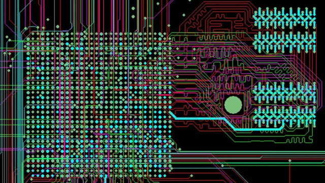
The PCB stack-up structure determines many electrical and mechanical characteristics of the final board.
For multilayer PCBs, engineers should carefully define:
- Signal layer arrangement
- Power and ground plane distribution
- Dielectric thickness
- Copper thickness
- Material selection
A proper stack-up design helps achieve:
- Stable impedance control
- Better signal integrity
- Reduced electromagnetic interference (EMI)
- Improved mechanical reliability
For high-speed and RF applications, stack-up planning should be completed before detailed routing begins.
2. Pay Attention to Component Placement
Component placement directly affects PCB performance and manufacturability.
During placement, engineers should consider:
Functional Grouping
Components belonging to the same functional circuit should be placed together to reduce routing complexity.
Examples:
- Power supply section
- Analog circuit section
- Digital processing section
- RF module section
Signal Flow Optimization
The layout should follow the signal transmission path to minimize unnecessary routing distance.
Shorter signal paths help reduce:
- Signal delay
- Noise coupling
- Transmission loss
Thermal Considerations
Heat-generating components should be positioned with sufficient space for heat dissipation.
Important components include:
- Power ICs
- Voltage regulators
- High-current devices
Proper placement improves thermal performance and product reliability.
3. Ensure Signal Integrity in High-Speed PCB Design
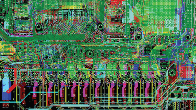
As signal frequencies increase, PCB traces behave more like transmission lines.
Designers should consider:
Controlled Impedance
High-speed signals require accurate impedance control.
Important parameters include:
- Trace width
- Copper thickness
- Dielectric thickness
- Material dielectric constant
Applications requiring strict impedance control include:
- High-speed communication systems
- RF circuits
- Semiconductor test boards
Differential Pair Routing
Differential signals are widely used for high-speed transmission.
Design considerations include:
- Matching trace length
- Maintaining consistent spacing
- Avoiding unnecessary vias
- Keeping reference planes continuous
Proper differential routing helps reduce noise and improve signal quality.
4. Optimize Power Distribution Design
Power integrity is another important consideration in PCB design.
A poor power distribution network may cause:
- Voltage fluctuations
- Excessive noise
- Component instability
Design practices include:
Proper Power and Ground Planes
Dedicated power and ground layers can provide:
- Lower impedance paths
- Better current distribution
- Reduced electromagnetic interference
Decoupling Capacitor Placement
Decoupling capacitors should be placed close to power pins.
This helps:
- Reduce power noise
- Stabilize voltage supply
- Improve high-frequency performance
5. Consider Electromagnetic Compatibility (EMC)
EMC performance should be considered during PCB design rather than after production problems occur.
Important practices include:
Minimize Current Loop Areas
Large current loops can increase electromagnetic radiation.
Designers should:
- Keep return paths short
- Maintain continuous ground planes
- Optimize power routing
Separate Noisy and Sensitive Circuits
High-noise circuits should be isolated from sensitive signal areas.
Examples:
- Switching power supplies
- Motor control circuits
- RF transmit sections
Proper separation reduces interference risks.
6. Design for Manufacturing (DFM)
A PCB design must not only work electrically but also be manufacturable.
DFM considerations include:
Trace Width and Spacing
Design rules should consider manufacturing capability.
Improper spacing may result in:
- Short circuits
- Open circuits
- Production yield reduction
Via Design
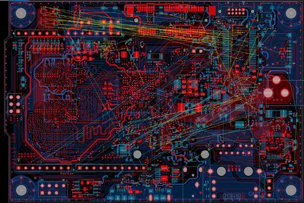
Engineers should consider:
- Via size
- Via aspect ratio
- Via placement
- Via reliability
Improper via structures may create fabrication difficulties.
Assembly Requirements
PCB design should consider:
- Component package selection
- SMT assembly limitations
- Inspection requirements
- Testing accessibility
Early DFM review helps identify potential production issues before fabrication.
7. Pay Attention to Thermal Management
Heat management is essential for reliable PCB operation.
Thermal design considerations include:
- Copper area optimization
- Thermal vias
- Heat dissipation paths
- Component spacing
Poor thermal design may lead to:
- Component aging
- Performance degradation
- Reduced product lifetime
8. Design for Testing and Maintenance
Testing capability should be considered during PCB design.
Important aspects include:
Test Point Arrangement
Adequate test points support:
- Electrical testing
- Debugging
- Production inspection
Accessibility Considerations
Designers should ensure important circuits can be easily tested and repaired.
This improves:
- Production efficiency
- Troubleshooting speed
- Maintenance convenience
9. Select Appropriate PCB Materials
Material selection affects PCB performance in different applications.
Considerations include:
- Operating frequency
- Temperature environment
- Mechanical requirements
- Electrical characteristics
Examples:
- Standard FR-4 for general applications
- Low-loss laminates for high-frequency circuits
- Flexible materials for FPC applications
Selecting the right material during early design helps avoid reliability issues later.
10. Perform Design Review Before Manufacturing
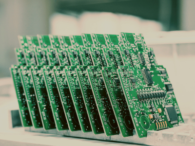
Before PCB fabrication, a comprehensive design review is essential.
The review should include:
- Electrical rule checking (ERC)
- Design rule checking (DRC)
- Signal integrity analysis
- Stack-up verification
- DFM analysis
Early review helps reduce:
- Prototype failures
- Manufacturing delays
- Additional redesign costs
Conclusion
PCB design is a comprehensive engineering process involving electrical performance, mechanical structure, manufacturing feasibility, and reliability considerations.
From stack-up planning and component placement to signal integrity control, thermal management, and DFM optimization, every design decision can influence the final product performance.
By considering these key precautions during PCB development, engineers can reduce design risks, improve production efficiency, and create more reliable PCB solutions for various applications.
