In modern electronics, PCB ESD design (Electrostatic Discharge design) is critical for ensuring product reliability and compliance with international standards. As circuits become more sensitive and densely integrated, improper ESD protection in PCB design can lead to catastrophic failures, latent defects, and reduced product lifespan.
Drawing from practical engineering experience, this guide explores real-world PCB ESD design techniques, focusing on ESD protection circuits, PCB layout strategies, grounding methods, and component selection to improve ESD robustness in PCB systems.
What Is ESD in PCB Design?
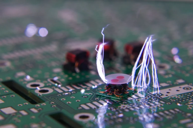
Electrostatic Discharge (ESD) is a sudden transfer of electrostatic charge between objects with different electrical potentials. In PCB systems, ESD events can damage components, disrupt signals, and degrade signal integrity.
Common ESD sources:
- Human contact (HBM – Human Body Model)
- Charged devices (CDM – Charged Device Model)
- Environmental electrostatic buildup
Effective PCB ESD protection design must address these real-world risks.
Why PCB ESD Design Is Critical
Proper ESD design in PCB layout ensures:
- Protection of sensitive ICs and interfaces
- Compliance with standards (IEC 61000-4-2)
- Improved product reliability and durability
- Reduced field failure rates
- Enhanced EMI/EMC performance
Without proper ESD protection PCB design, even a small discharge can cause permanent damage.
Core Principles of PCB ESD Design
1. Provide a Low-Impedance Discharge Path
The primary goal of ESD PCB design is to safely divert ESD current away from sensitive components.
Best practices:
- Design short, wide traces for ESD paths
- Connect ESD paths directly to ground
- Minimize inductance in discharge routes
2. Proper Grounding Strategy
A robust grounding design in PCB ESD protection is essential.
Techniques:
- Use solid ground planes
- Avoid split ground under ESD paths
- Apply via stitching to reduce impedance
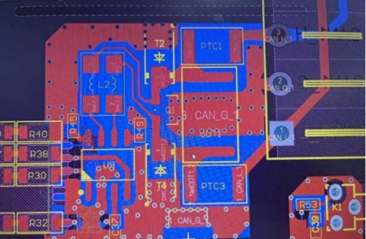
3. Component-Level ESD Protection
Selecting proper ESD protection devices enhances system resilience.
Common components:
- TVS diodes (Transient Voltage Suppression)
- ESD protection arrays
- Ferrite beads for noise suppression
Place these components close to external connectors in PCB layout design.
4. Interface and Connector Protection
External interfaces are the most vulnerable points in PCB ESD design.
Design recommendations:
- Place ESD protection devices near connectors
- Route signals from connector → protection device → IC
- Avoid long traces before protection components
5. Trace Routing and Layout Optimization
Proper PCB routing design for ESD protection reduces risk.
Key rules:
- Keep ESD-sensitive traces short
- Avoid routing near board edges
- Maintain spacing between high-risk nodes
6. Layer Stack-Up and Shielding
Optimized PCB stack-up design improves ESD immunity.
Approaches:
- Place signal layers adjacent to ground planes
- Use shielding layers for sensitive circuits
- Separate analog, digital, and high-speed sections
Advanced PCB ESD Design Techniques
1. Guard Rings and Ground Shielding
Using guard rings around sensitive circuits helps isolate ESD events.
2. Series Resistors and Filtering
Adding small resistors or RC filters reduces ESD energy reaching ICs.
3. Transient Current Loop Minimization
Design compact current loops to reduce inductive voltage spikes.
4. Edge Protection Design
Avoid placing critical components near PCB edges where ESD is more likely to occur.
Common PCB ESD Design Mistakes
- Placing ESD protection devices too far from connectors
- Using narrow traces in ESD paths
- Poor grounding and high impedance return paths
- Ignoring ESD in early PCB layout design stages
- Overlooking system-level ESD testing
Avoiding these mistakes significantly improves PCB ESD protection performance.
ESD Testing and Standards
To validate PCB ESD design, products must undergo testing such as:
- IEC 61000-4-2 ESD immunity testing
- Contact discharge and air discharge tests
- System-level ESD validation
Testing ensures compliance and reliability in real-world environments.
Applications of PCB ESD Design
Effective ESD protection PCB design is critical in:
- Consumer electronics (smartphones, laptops)
- Industrial control systems
- Automotive electronics
- Medical devices
- Communication equipment
Conclusion
Practical PCB ESD design requires a combination of proper grounding, optimized layout, effective protection components, and real-world testing. By implementing proven ESD protection techniques in PCB design, engineers can significantly enhance product reliability, reduce failures, and ensure compliance with industry standards.
A well-executed ESD protection strategy in PCB layout is essential for modern high-performance electronic systems.
