In the Texas Instruments technical article, “How low-power 60GHz mmWave radar sensors enable high-precision sensing in more applications,” we discussed how 60GHz millimeter-wave (mmWave) radar sensors enable high-precision sensing in industrial and consumer electronics applications. In this article, we will explore how low-power 77GHz radar sensors can help achieve reliable and accurate sensing in other challenging applications....
HomeAuthor
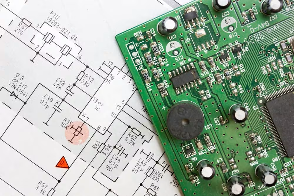
kkpcba-Cindy - KKPCB - Page 12 of 66
Understanding the Foundation of PCB Technology A Printed Circuit Board (PCB) is the foundation of nearly every modern electronic product. From: consumer electronics industrial automation systems automotive electronics medical devices aerospace communication equipment high-speed networking hardware PCBs provide the essential platform for: electrical connectivity signal transmission component mounting power distribution As electronic products continue...
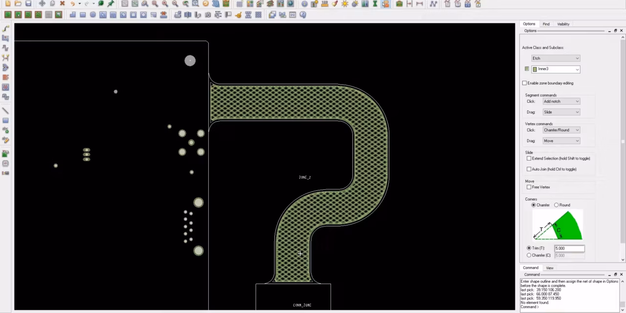
Key Takeaways Cross-hatching significantly increases the flexibility of flex PCBs by reducing copper content. Helps maintain optimal impedance in flex PCBs without altering dielectric thickness or signal line width. Enables efficient manufacturing with reduced copper usage and improved resin adhesion. Cross-hatch PCB connector PCB cross-hatching is a technique where certain planes or large copper areas are designed...
Master Your Budget: Proven Strategies for Rigid Flex PCB Cost Optimization In modern electronics, Rigid-Flex PCB technology is the gold standard for compact, high-reliability designs. However, the complexity of Rigid-Flex manufacturing often leads to higher production expenses. Achieving effective Rigid Flex PCB cost optimization requires a strategic balance between sophisticated engineering and smart logistical choices. At KKPCB, we help engineers navigate these...
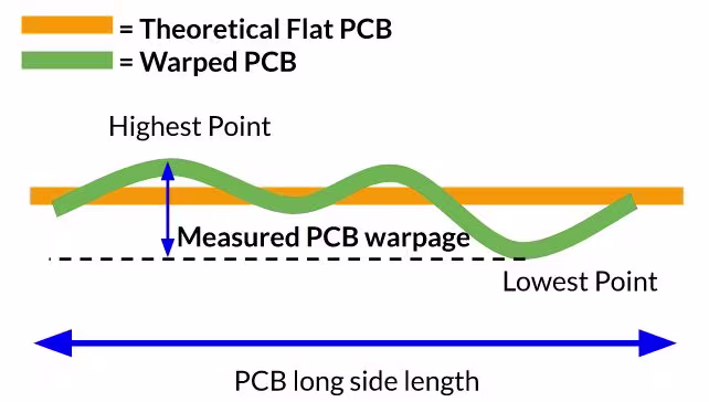
Key Takeaways Stress during fabrication, such as thermal expansion and contraction, imbalanced copper distribution, and improper handling, can lead to warpage. Utilize tools like feeler gauges, height gauges, contour gauges, optical profilometers, and Finite Element Method (FEM) simulations to accurately measure PCB warpage. Effective design practices using OrCAD X, such as symmetrical component placement and...
PCB DesignCustomer CaseElectronics Industry NewsEngineering TechnologiesPCB Assembly (PCBA)PCB Manufacturing
How to Create a Variable Power Supply PCB Layout
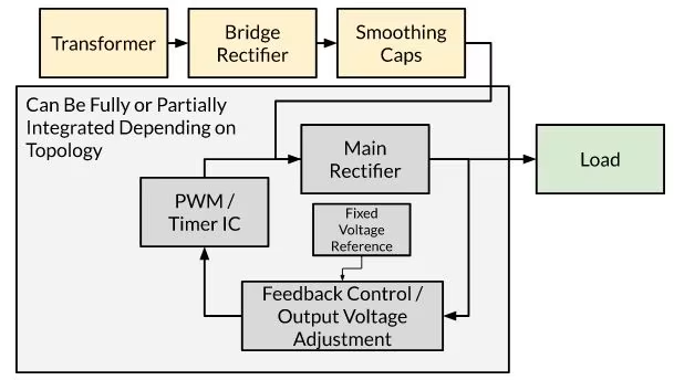
A variable power supply PCB is one of the most essential designs in electronic engineering, lab equipment, industrial systems, and embedded development platforms. It allows adjustable output voltage and current, making it suitable for testing, prototyping, and powering sensitive circuits. Designing a reliable variable power supply PCB layout requires careful consideration of power integrity, thermal...
Key Takeaways The competitiveness of new product introduction makes it critical to optimize your prototype design process for effectiveness and efficiency. Your prototype PCB design software should exhibit essential attributes for managing component inventory, creating schematics, designing PCBs, verifying designs, and managing data. OrCAD X delivers the essential functionality and capabilities in one program for prototype design...
PCB design involves two critical stages: component layout and circuit connection wiring. The layout is the arrangement of circuit components within the PCB’s wiring area. A well-thought-out layout directly affects the ease of subsequent wiring and significantly impacts the PCB’s overall performance. In addition to meeting circuit functionality and performance requirements, a good layout considers manufacturability, inspection, and maintenance....
Electromagnetic compatibility (EMC) refers to the ability of electronic devices to function harmoniously in their electromagnetic environment without causing or being affected by electromagnetic interference (EMI). The goal of EMC design is to enable electronic devices to resist external interference while minimizing the electromagnetic interference they emit to surrounding devices. 1. Selecting the Right Wire Width Minimizing inductance...
Printed Circuit Board (PCB) design is a critical step in the development of any electronic product. A well-designed PCB ensures reliability, performance, and manufacturability, while a poor design can lead to costly failures and delays. Below are five golden rules that every PCB designer should follow. 1. Prioritize Clear and Logical Layout A clean and...
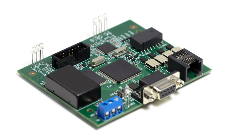
KKPCB is a leading electronic solutions provider specializing in PCB design, fabrication, assembly, and testing for Flex, Rigid-Flex, RF/Microwave, HDI, rigid multilayer, and ATE test boards. We offer comprehensive end-to-end services, including prototyping, component sourcing, SMT/THT assembly, functional testing, enclosure assembly, and final product packaging. With our one-stop, in-house capabilities, KKPCB delivers OEM and ODM solutions with fast turnaround, high quality, and cost-effective results, serving clients worldwide.

PCB Manufacturing
PCB Assembly
Technical Support