
HomeTag

Sequential lamination - KKPCB

Blind & Buried Vias in HDI PCB: Design & Manufacturing Expertise

Blind and Buried Vias in HDI PCB Design: Engineering Principles, Manufacturing Constraints, and KKPCB’s Advanced Capabilities As high-density interconnect (HDI) technology becomes essential in 5G, wearables, automotive radar, aerospace, and compact IoT systems, PCB designers increasingly rely on blind vias and buried vias to meet aggressive space, performance, and reliability requirements. These via structures allow...
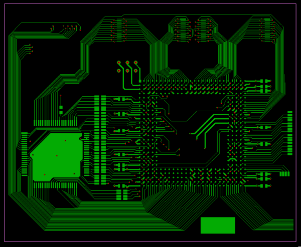
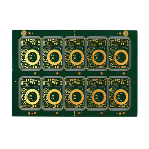
Buried Via PCBs: Advanced Techniques for High-Density Multilayer Boards

Buried via technology has become essential in modern PCB design, particularly for high-density, high-performance applications. Unlike through-hole vias that pass through all layers, buried vias connect only internal layers, leaving outer layers uninterrupted. This allows designers to maximize routing space, improve signal integrity, and achieve compact, multilayer PCB layouts. Design Advantages Maximizing Board Real Estate:By...

Blind and Buried Vias in PCB Design – Advanced HDI Interconnection Solutions

Blind and Buried Vias in PCB Design — Structure, Function, and Manufacturing Insights As the miniaturization of electronic components continues to accelerate, PCB designs must accommodate finer pitch components and higher circuit densities, especially in advanced mobile, communication, and computing applications. One of the critical technologies enabling this evolution is the use of blind and...