RF PCB - KKPCB
 
HomeTag

RF PCB - KKPCB

Buy High Frequency PCBs Optimized for Controlled Impedance and Low Insertion Loss in 5G and Satellite Systems

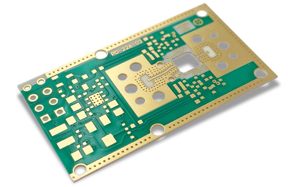
As 5G wireless infrastructure and satellite communication systems continue to evolve toward higher frequencies, wider bandwidths, and denser integration, the demand to buy high frequency PCBs with precise electrical control has increased significantly. In these applications, controlled impedance PCB design and ultra-low insertion loss PCB performance are no longer optional—they are fundamental to achieving stable...

Designing Buried Via PCBs for High-Density Routing and Signal Integrity Optimization

As electronic systems continue to evolve toward higher speeds, smaller form factors, and increased functionality, traditional through-hole via structures are becoming a limiting factor. Buried Via PCB technology has emerged as a key solution for achieving high-density routing and optimizing signal integrity, especially in HDI, high-speed digital, and RF designs. By embedding vias between internal...

Controlled Impedance PCB Engineering for High-Speed Digital and High-Frequency RF Applications

A Controlled Impedance PCB is a critical foundation for modern high-speed digital systems and high-frequency RF applications. As signal rise times shrink and operating frequencies extend into multi-GHz ranges, PCB interconnects must behave as predictable transmission lines rather than simple copper connections. Controlled Impedance PCB design ensures signal integrity, phase stability, and EMI compliance across...

High-Stability Double Layer HF PCB Engineering for Low-Loss RF Routing and Precision High-Frequency Performance

A Double Layer HF PCB is one of the most efficient and cost-optimized architectures for high-frequency designs requiring low-loss transmission, tight impedance control, and stable RF performance up to microwave and lower mmWave ranges. Compared with complex multilayer structures, the Double Layer HF PCB offers a cleaner electromagnetic environment, reduced dielectric loading, and minimized stackup...

Advanced RF Engineering with Duroid 6010 PCB: Ultra-High-Dk Performance for Microwave, Radar, and Aerospace Systems

Introduction: Why Duroid 6010 PCB Is a Cornerstone of High-Frequency Engineering Rogers Duroid 6010 PCB is one of the most widely used materials for extreme high-frequency and microwave systems requiring exceptionally high dielectric constant and low loss.With a Dk of approximately 10.2, the Duroid 6010 PCB platform enables dramatic circuit miniaturization, enhanced electromagnetic coupling, and...

Duroid 6010 PCB Engineering: Ultra-High Dielectric, Low-Loss Design for RF, Microwave, and Aerospace Systems

Duroid 6010 PCB, based on Rogers RT/duroid® 6010LM material, is one of the most critical substrates used in microwave, RF, aerospace, satellite, and defense systems. Known for its ultra-high dielectric constant (Dk ≈ 10.2) and extremely low dissipation factor, Duroid 6010 PCB enables the miniaturization of RF paths, improved resonator stability, and enhanced signal precision...

Engineering Duroid 6010 PCB for Extreme High-Frequency, Low-Loss, and Ultra-Stable Microwave Applications

As microwave, satellite, radar, and millimeter-wave systems move deeper into high GHz operating regions, engineers require PCB materials with ultra-stable dielectric behavior, extremely high Dk, and exceptionally low loss. This is where Duroid 6010 PCB—based on Rogers RT/duroid® 6010LM—becomes a foundational choice for critical RF and microwave engineering. With a dielectric constant (Dk) of ~10.2,...

Engineering Double Layer HF PCB for Ultra-Stable RF Performance and Low-Loss Microwave Signal Integrity

As RF communication, IoT edge devices, automotive radar, and compact wireless modules continue to evolve, the Double Layer HF PCB has become a preferred architecture for delivering high-frequency stability, low insertion loss, and predictable electromagnetic performance. Although limited to two copper layers, a Double Layer HF PCB—when engineered correctly—can outperform many multilayer structures in signal...

Engineering Ultra-Low Loss Performance with Low Dissipation Factor PCB Materials for High-Frequency and High-Speed Systems

Low Dissipation Factor PCB Engineering for High-Frequency, High-Power, and Low-Loss Electronic Platforms A Low Dissipation Factor PCB is the backbone of modern high-frequency hardware, designed to minimize dielectric loss, reduce signal attenuation, and maintain stable RF performance across extreme bandwidths. As systems scale into mmWave, sub-THz, and multi-gigabit domains, the dissipation factor (Df) becomes a...

PCB Prototype Engineering: Achieving High Reliability, High Speed, and High Precision in Modern Electronics

Introduction: Why PCB Prototype Engineering Defines Modern Electronics A PCB Prototype is no longer just a pre-production sample—it is the central engineering stage that determines product performance, manufacturability, reliability, and cost.In advanced electronics such as 5G, IoT, robotics, automotive, aerospace, AI edge computing, and industrial automation, a well-engineered PCB Prototype ensures signal integrity, thermal stability,...