RF PCB - KKPCB
 
HomeTag

RF PCB - KKPCB

Enhance Signal Integrity and High-Speed Stability with Impedance Controlled PCB Platforms for 5G Communication Systems

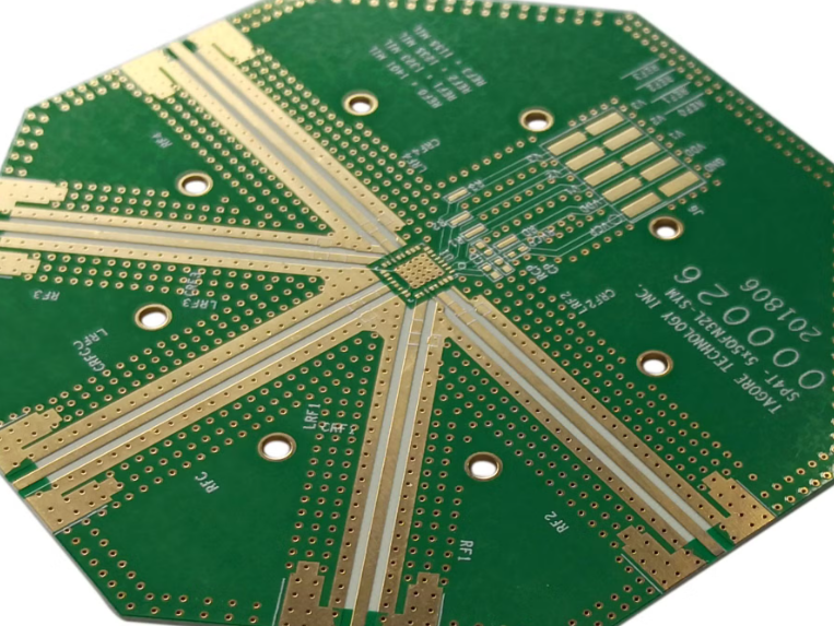
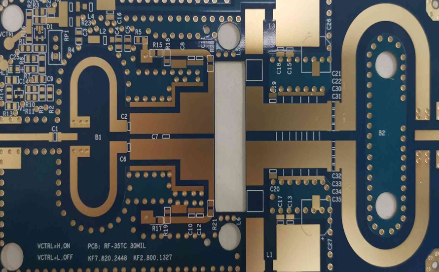
5G communication systems rely on stringent impedance accuracy, low insertion loss, and predictable phase stability to maintain signal integrity across multi-gigabit transmission channels. At mmWave and sub-6 GHz bands, even slight deviations in controlled impedance routing can introduce reflection, jitter accumulation, and eye-diagram degradation.Impedance Controlled PCBs engineered for 5G must balance dielectric uniformity, copper surface...

Optimize RF Transmission and Phase Consistency Using High-Frequency Sensor PCB Laminates in Automotive ADAS Sensing Modules

Next-generation automotive ADAS sensing modules, including 77–81 GHz radar, LiDAR, and mmWave sensor arrays, require PCBs with ultra-stable dielectric properties, low insertion loss, and phase-coherent RF routing. Performance depends on maintaining consistent Dk/Df, low-loss mmWave signal propagation, and minimal EMI, even under harsh thermal cycling, vibration, and humidity conditions in vehicles.   High-frequency sensor PCB...

Enhance Signal Integrity and Thermal Reliability with ADAS PCB Platforms for Automotive Radar Systems

Advanced Driver Assistance Systems rely heavily on 77 GHz automotive radar modules, where the ADAS PCB directly determines signal integrity, insertion loss, dielectric stability, and system-level thermal reliability. As radar sensors expand from single-beam to multi-beam architectures, PCB materials and stackup selection have become primary constraints for RF linearity and long-distance object detection. The objective...

Enhance Thermal Reliability and High-Power RF Efficiency Through Advanced 5G Router PCB Stackups

5G router PCB platforms operate under multi-band RF loads, high-density routing, and continuous thermal cycling in compact CPE enclosures. Achieving stable RF efficiency requires a stackup engineered around low-loss materials, controlled dielectric stability, and carefully optimized thermal paths. This article analyzes how engineered 5G router PCB stackups improve RF efficiency, insertion-loss performance, and long-term thermal...

Optimizing High-Frequency Stability and Low-Loss Transmission Using RF-35 PCB Laminates for Modern Wireless Systems

RF-35 PCB laminates operate in a class where dielectric precision directly shapes RF linearity, bandwidth uniformity, and system-level efficiency. Modern wireless products—Wi-Fi 6/7 modules, IoT gateways, sub-6 GHz links, and microwave-band transceivers—depend on stable Dk/Df behavior to maintain predictable impedance and low insertion loss. RF-35 offers a low-loss dielectric platform designed for controlled RF propagation,...

High-Frequency Signal Integrity Optimization and Phase-Stable Transmission with Megtron 7 PCB Substrates in 5G Server and High-Speed Computing Systems

Megtron 7 PCB laminates are widely adopted in 5G servers, AI computing accelerators, and cloud networking equipment due to their exceptionally low dielectric loss and superior stability at 28–112 Gbps PAM4 and mmWave bands. As system architectures transition toward high-density multi-lane SerDes and advanced RF interconnects, PCB materials become a primary constraint influencing channel loss...

High-frequency Wi-Fi 6/7 antenna modules in modern laptops demand PCBs that maintain low insertion loss, precise phase alignment, and robust EMI suppression within compact layouts. TLY-5 PCB laminates, with a dielectric constant of 3.45 ± 0.03 and dissipation factor of 0.0012 @10 GHz, provide low-loss RF transmission and dimensional stability essential for multi-band performance. KKPCB...

Low-Loss Transmission and EMI Control of Ceramic PCBs in Satellite Communication and High-Frequency Payload Units

Engineering Context / Abstract   In modern satellite communication systems, RF payload units demand precise signal transmission, minimal insertion loss, and robust EMI suppression. High-frequency payloads, including Ku- and Ka-band transceivers, operate under extreme thermal, vacuum, and radiation conditions, where even minor dielectric fluctuations can cause phase errors and signal degradation.   Ceramic PCB substrates,...

High-Density Power Integrity and Heat Dissipation Optimization Using Ceramic PCB Substrates in Laptop Motherboards and Wi-Fi 7 Systems

Engineering Context / Abstract   Modern laptop motherboards and Wi-Fi 7 modules demand exceptional power integrity and efficient thermal management due to the increasing density of integrated circuits, high-speed memory buses, and advanced RF front-end modules. Ceramic PCB substrates, featuring low dielectric loss (Df = 0.0015 @10GHz) and stable dielectric constant (Dk = 9.8 ±...

Low Loss PCBs Explained: Materials, Features & High-Frequency Performance

What Is a Low Loss PCB? Premium Materials, Performance Advantages & Applications In high-frequency electronics, signal integrity is everything. As data rates climb and RF systems move into the mmWave range, traditional FR-4 PCBs quickly become inadequate due to excessive dielectric loss, copper loss and thermal instability. At KKPCB, we engineer Low Loss PCBs specifically...