PCB Design - KKPCB
 
HomeTag

PCB Design - KKPCB

ADAS PCB Layout Guidelines for Automotive Radar Systems: Best Practices for High-Frequency Design

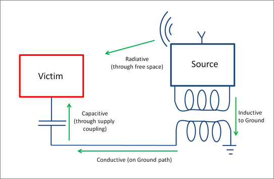
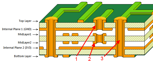
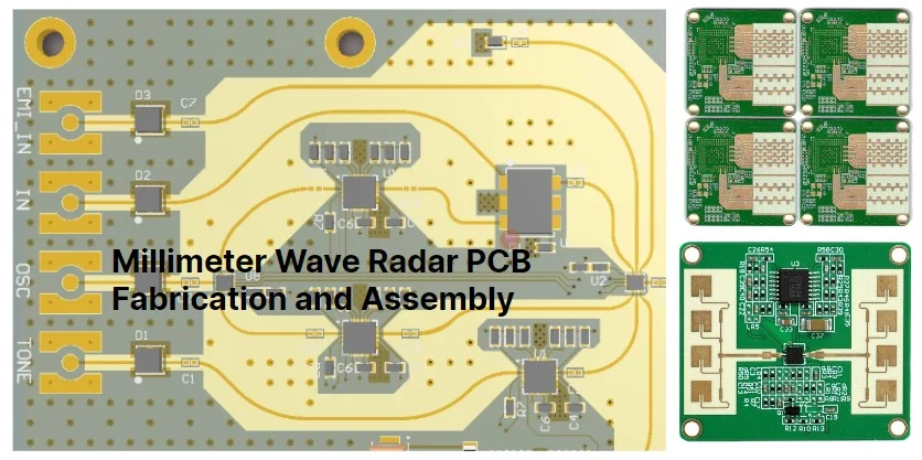
ADAS PCB Layout Guidelines for Automotive Radar Systems In the rapidly advancing world of automotive technology, Advanced Driver Assistance Systems (ADAS) are revolutionizing how we drive, enhancing safety and intelligence in vehicles. At the heart of many ADAS features lies the automotive radar system, which relies on precise and effective printed circuit board (PCB) design...

PCB Design Guidelines for EMC Compliance

Why EMC Matters in PCB Design Electromagnetic Compatibility (EMC) is a key requirement in modern PCB design, ensuring that electronic systems operate reliably without generating or being affected by electromagnetic interference (EMI). Proper PCB layout—especially GND routing, trace spacing, and layer design—plays a decisive role in reducing ESD (Electrostatic Discharge) and improving overall signal integrity....

Why Should Vias Be Staggered from Pad Positions in PCB Design?

 The Importance of Via Placement in PCB Design In PCB design, via positioning plays a crucial role in ensuring electrical performance, manufacturing reliability, and signal integrity. Improper via placement—especially placing vias directly on component pads—can lead to soldering defects, electrical noise, and higher production costs. This article explains why vias should be staggered from pad...

PCBs for Industrial Automation: The Backbone of Modern Control Systems

PCBs for Industrial Automation: The Backbone of Modern Control Systems In the fast-evolving world of industrial automation, Printed Circuit Boards (PCBs) are the unsung heroes that power the technology behind every automated machine, robot, and control system. From factory floors to advanced robotics, choosing the right PCB is crucial to the success of your automation...

Mastering High-Speed PCB Test Point Design: Precision, Performance, and Signal Integrity

Mastering High-Speed PCB Test Point Design: Precision, Performance, and Signal Integrity In high-speed printed circuit board (PCB) design, test point placement is far more than a routine step—it’s a science of balance. The miniature metal pads scattered across a PCB may look simple, but their position, size, and electrical behavior can determine whether a product...

Explore how KKPCB engineers world-class radar PCBs for automotive, aerospace, and defense applications. Learn about design techniques, RF materials, and manufacturing precision for frequencies up to 77 GHz.

Radar PCB Overview Radar PCBs represent the pinnacle of high-frequency circuit design, bridging advanced RF engineering and precise manufacturing. These specialized boards operate in the 1 GHz – 77 GHz range, demanding exceptional signal integrity, low loss materials, and extreme reliability — especially in mission-critical applications like automotive radar, aerospace, and defense. KKPCB has extensive...

PCB Design Best Practices: Key Considerations for Optimized Performance

When designing printed circuit boards (PCBs), a well-structured approach and attention to detail are essential to ensure functionality and avoid potential design errors. Here are some key PCB design tips based on practical experience: 1. Pay Attention to Pin Definitions and Package Names in the Schematic Library When creating the schematic library, ensure that each schematic pin corresponds correctly...