KKPCB Engineering - KKPCB
 
HomeTag

KKPCB Engineering - KKPCB

Designing High Layer Count PCBs for Complex Signal, Power, and Thermal Integrity Challenges

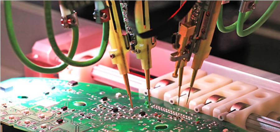
As electronic systems continue to integrate higher data rates, greater power density, and tighter form factors, high layer count PCBs have become a foundational platform for modern hardware architecture. Designs exceeding 16, 20, or even 30 layers are now common in data center equipment, telecommunications infrastructure, aerospace electronics, and industrial control systems. However, increasing layer...

Engineering Precision: The Critical Role of Probe Card PCBs in Semiconductor Testing

Engineering Precision: The Critical Role of Probe Card PCBs in Semiconductor Testing Introduction In semiconductor production, precision defines success. Every chip must be verified for performance and reliability before it’s packaged—and the key to this process lies in the probe card PCB.At KKPCB, we specialize in engineering high-performance probe card PCBs that ensure accurate, repeatable,...

About PCB Layer Stackup

A PCB Layer Stackup refers to the arrangement of conductive copper layers and insulating dielectric materials that make up a multilayer PCB. In the era of high-speed digital electronics and 5G, the stackup is no longer just a mechanical carrier; it is a critical tool for managing signal integrity, power distribution, and electromagnetic compatibility (EMC). A well-engineered stackup from KKPCB ensures...