IoT PCB - KKPCB
 
HomeTag

IoT PCB - KKPCB

Fine Line PCB: High-Density, Precision PCB Solutions for Advanced Electronics

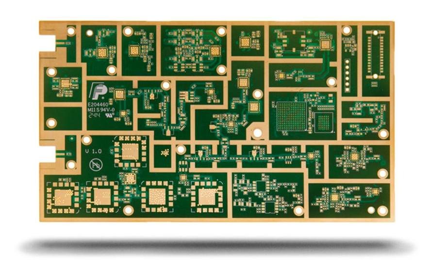
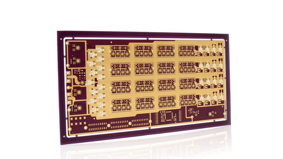
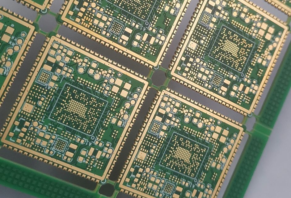
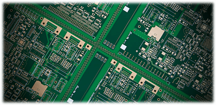
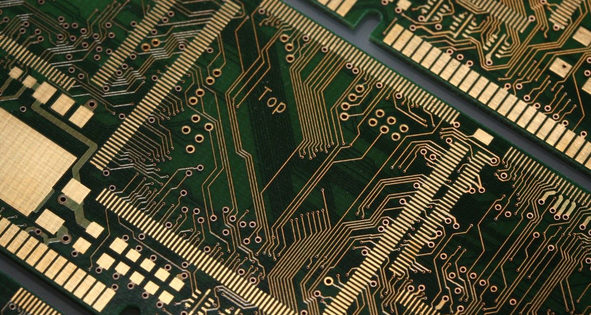
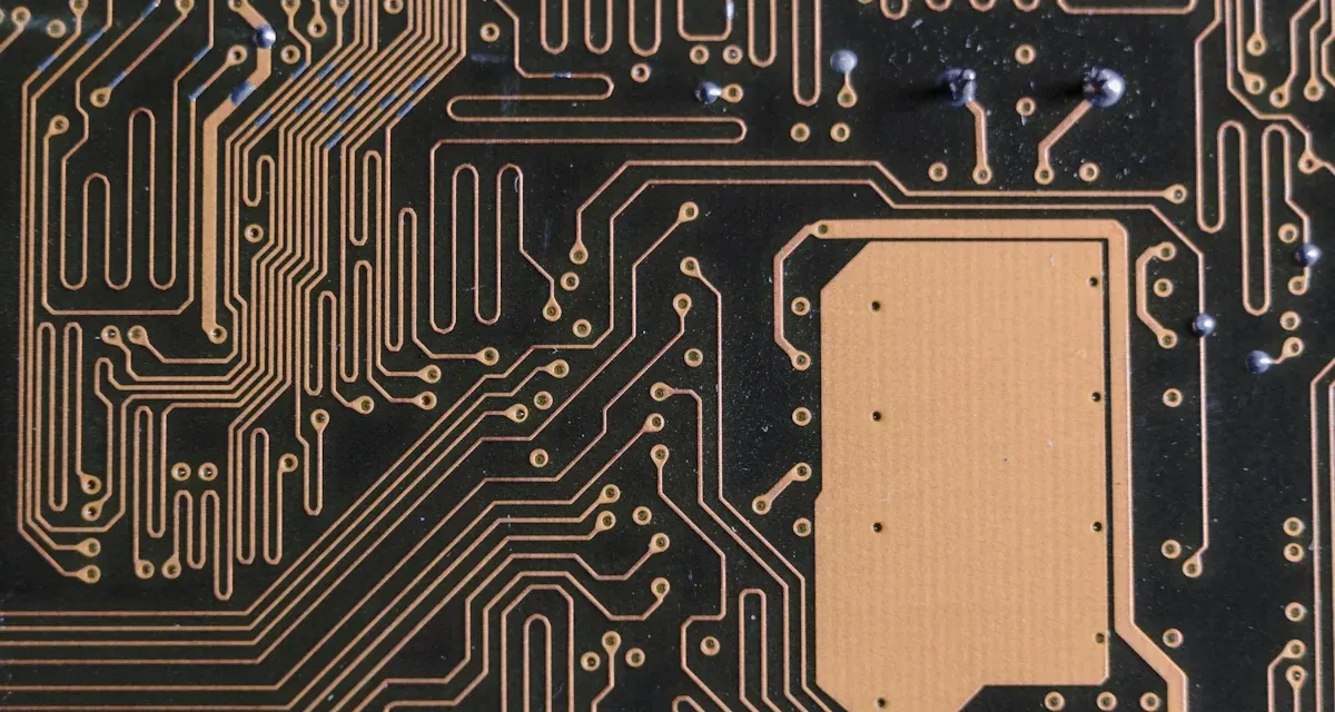
What Is a Fine Line PCB? A Fine Line PCB is a printed circuit board engineered with ultra-narrow traces and tight spacing, typically below 100 µm. This enables high-density routing and compact component placement while maintaining excellent signal integrity and reliability. Fine line PCBs are essential in high-speed digital systems, RF modules, 5G devices, IoT...

Low Loss PCB: Advanced PCB Technology for High-Speed, RF, and High-Frequency Applications

A Low Loss PCB is a specialized printed circuit board designed to reduce dielectric loss, insertion loss, and signal distortion in high-speed and high-frequency electronic systems. As modern electronics such as 5G communication systems, RF front-end modules, high-speed data transmission, and semiconductor test equipment operate at ever-increasing frequencies, signal integrity becomes a critical design challenge....

Thermal Management PCB: Optimized Heat Dissipation Solutions for High-Power Electronics

A Thermal Management PCB is a specialized printed circuit board engineered to effectively manage heat generation in electronic systems. As devices such as automotive ECUs, 5G modules, RF circuits, power electronics, and industrial IoT devices operate at higher power densities, efficient heat dissipation becomes critical to maintain performance, reliability, and lifespan. Key Features of Thermal...

Multilayer PCB: Advanced Solutions for High-Density and High-Performance Electronics

A Multilayer PCB is a printed circuit board composed of three or more layers of conductive traces separated by insulating substrates, allowing more complex circuitry, higher routing density, and superior signal integrity. Multilayer PCBs are widely used in high-speed computing, RF communication, IoT, semiconductor testing, and automotive systems, where compact size and high performance are...

Low Loss PCB: High-Performance Solutions for RF, 5G, and High-Speed Electronics

A Low Loss PCB is a specialized printed circuit board engineered to minimize signal attenuation, dielectric loss, and crosstalk in high-speed, high-frequency, and RF electronic systems. With the rise of 5G, IoT, high-speed computing, and advanced semiconductor testing, ensuring signal integrity and reliable performance is more critical than ever. Key Features of Low Loss PCBs...

Fine Pitch PCB: Precision Solutions for High Pin Count and Miniaturized Electronics

A Fine Pitch PCB is a printed circuit board designed to support high-density integrated circuits with extremely small pad spacing, such as BGA, QFN, CSP, and flip-chip packages. As modern electronics continue to shrink in size while increasing functionality, fine pitch PCB technology becomes essential for achieving high routing density, reliable assembly, and superior electrical...

High Density PCB: Advanced Solutions for Compact and High-Performance Electronics

A High Density PCB (HDPCB) is a printed circuit board designed to support compact, high-performance electronic systems. By leveraging HDI technology, microvias, blind/buried vias, and multilayer stackups, high density PCBs allow engineers to integrate more functionality into smaller footprints, making them essential for smart devices, high-speed computing, RF communication, and semiconductor testing. Key Features of...

High Density PCB: Advanced Design and Manufacturing for Compact and High-Performance Electronics

A High Density PCB (HDPCB) is a specialized printed circuit board designed for compact, high-performance, and high-pin-count electronic applications. HD PCBs are widely used in semiconductor test boards, IoT devices, wearable electronics, automotive systems, and high-speed communication modules, where space constraints, signal integrity, and reliability are critical. High density PCBs combine fine-pitch component layouts, multilayer...

Fine Pitch PCB: Precision PCB Solutions for High-Density Component Integration

A Fine Pitch PCB is a specialized printed circuit board designed for high-density ICs and compact electronic systems. Fine pitch technology supports components with very small pad spacing, allowing engineers to place high pin count ICs in limited PCB areas without compromising electrical performance. Fine pitch PCB design is crucial for modern applications like 5G...

High Density PCB: Advanced PCB Solutions for Compact, High-Performance Electronics

A High Density PCB (HDPCB) is a multilayer, fine-pitch printed circuit board designed to support compact electronic devices, high-speed digital systems, and high-frequency applications. HDPCBs are widely used in telecommunications, 5G, IoT, automotive electronics, and high-performance computing, where space constraints, high pin counts, and advanced signal integrity requirements demand precise PCB engineering. High density PCB...