Impedance Controlled PCB - KKPCB
 
HomeTag

Impedance Controlled PCB - KKPCB

Maximize mmWave Performance and Thermal Stability with RO5880 PCB Laminates in Next-Generation RF and Satellite Systems

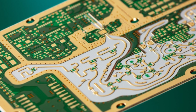
High-frequency RF and satellite systems increasingly demand mmWave operation with extreme signal fidelity, low insertion loss, and precise phase alignment. RO5880 PCB laminates (Dk = 2.2 ± 0.02, Df = 0.0009 @10 GHz) provide ultra-low dielectric loss and superior thermal stability, ensuring consistent high-frequency propagation across multilayer stackups. KKPCB employs advanced multilayer RO5880 PCB stackups,...

Design Next-Gen Satellite Communication Systems with RO4835 PCB for Precise Impedance Control and Wideband Consistency

Satellite communication systems require ultra-stable RF performance across wide frequency bands, often spanning Ka- and Ku-bands. Maintaining precise impedance control, minimal insertion loss, and consistent phase response is critical for antenna feeds, transceivers, and payload modules. RO4835 PCB laminates (Dk = 3.48 ± 0.03, Df = 0.0037 @10 GHz) offer low-loss, thermally stable dielectric properties,...

Achieve Phase-Stable Multi-Gigabit Routing with Low Loss PCB Stackups for High-Speed Data Center Networks

Modern data center networks depend on multi-gigabit signal transmission, low-latency switching, and phase-coherent high-speed channels. As switching fabrics migrate from 25G/40G toward 100G/200G/400G architectures, even micro-scale distortions in dielectric properties or copper structures can degrade eye diagrams, reduce SNR, and trigger packet loss.This is why Low Loss PCB stackups—built with engineered dielectric materials and ultra-controlled...

Enhance Signal Integrity and Thermal Reliability in Multilayer Blind Via PCBs for High-Density RF Modules

High-density RF modules in 5G base stations, satellite payloads, and advanced IoT systems require compact multilayer PCBs with precise signal routing, minimal crosstalk, and high thermal resilience. Blind via technology allows for efficient vertical interconnects while reducing PCB stackup thickness, improving high-frequency performance, and maintaining signal integrity across densely packed layers. KKPCB integrates precision lamination,...

Optimize Beamforming Accuracy and Ultra-Low-Loss RF Propagation Using High-Frequency mmWave Module PCB Architectures for 28–60 GHz Wireless Platforms

High-frequency mmWave module PCB architectures define the performance boundary of 28–60 GHz wireless platforms, where beamforming accuracy, ultra-low-loss routing, and tight impedance control determine every detail of system efficiency. In dense phased-array units, even microscopic changes in Dk/Df, copper roughness, dielectric uniformity, or via transition geometry produce measurable degradation in beam steering vectors, noise floors,...

Improve Multi-Gigabit Transmission and Low-Loss Routing Through Impedance Controlled PCB Engineering for Data Center Switches

Modern data center switches demand high-speed, multi-gigabit transmission across densely packed PCB layers. Maintaining low insertion loss, tight impedance control, and minimal crosstalk is critical to guarantee reliable signal integrity, reduce latency, and preserve network throughput. Impedance-controlled PCB architectures provide predictable high-frequency performance for differential pair routing and dense multilayer stackups. KKPCB leverages precision lamination,...

Optimize RF Signal Integrity and Lightweight HDI UAV PCB Architectures for Next-Gen Drone Navigation Modules

Next-generation UAV systems—whether used for industrial IoT sensing, long-range inspection, autonomous mapping, or precision agriculture—depend on PCB platforms capable of delivering high-frequency RF accuracy, ultra-stable GNSS/GPS reception, multi-band communication reliability, and lightweight HDI construction. As flight durations extend and sensor payloads grow more complex, the PCB becomes the backbone that determines navigation precision, RF sensitivity,...

Optimize Thermal Resilience and Multi-Layer Signal Fidelity with Megtron 7 PCB Stackups in High-Performance Computing Modules

High-performance computing modules in data centers, AI accelerators, and HPC servers operate with dense multi-layer interconnects and high-frequency signaling. Signal degradation, thermal hotspots, and impedance drift can severely impact throughput and reliability. Megtron 7 PCB laminates offer low-loss dielectric properties, tight Dk/Df tolerances, and high thermal conductivity, enabling reliable high-speed signal transmission in complex multi-layer...

Achieve Ultra-Stable Dk/Df and Low-Loss Performance with RO4835 PCB Architectures for High-Density 5G Massive-MIMO Radio Units

Next-generation 5G massive-MIMO radio units require high-density PCB designs that maintain ultra-consistent dielectric constant (Dk) and dissipation factor (Df) across all layers. Any variation in Dk/Df can lead to impedance mismatches, phase errors, and RF signal degradation, negatively affecting beamforming accuracy and spectral efficiency. RO4835 PCB laminates (Dk = 3.48 ± 0.03, Df = 0.0037...

Optimize High-Frequency UAV PCB Architectures to Enhance IoT Crop Monitoring, Precision Spraying, and Long-Range Agricultural Drone Communication

IoT-enabled agricultural UAVs operate in a uniquely demanding environment: wide temperature swings, continuous vibration, variable humidity, and rapidly changing RF propagation conditions over open farmland. These drones must maintain long-range wireless links, collect high-resolution crop data, and execute precision-controlled spraying while keeping power consumption and mass as low as possible. To meet these requirements, modern...