Impedance Controlled PCB - KKPCB
 
HomeTag

Impedance Controlled PCB - KKPCB

Optimize High-Frequency UAV PCB Architectures to Enhance IoT Crop Monitoring, Precision Spraying, and Long-Range Agricultural Drone Communication

IoT-enabled agricultural UAVs operate in a uniquely demanding environment: wide temperature swings, continuous vibration, variable humidity, and rapidly changing RF propagation conditions over open farmland. These drones must maintain long-range wireless links, collect high-resolution crop data, and execute precision-controlled spraying while keeping power consumption and mass as low as possible. To meet these requirements, modern...

Boost RF Linearity and Phase Consistency with Impedance Controlled PCB Architectures in Aerospace Navigation and Telemetry Modules

Aerospace navigation and telemetry links depend on signals that simply cannot drift, distort, or wander off-phase. Whether guiding a launch vehicle or stabilizing a satellite’s inter-orbital communication, the RF path must maintain tight impedance control, predictable phase behavior, and ultra-low distortion across multi-GHz carriers. This is where Impedance Controlled PCB architectures become fundamental—not an optional...

Achieve Low-Loss Performance and Long-Term Stability Through ADAS PCB Materials for Multi-Sensor Fusion Modules

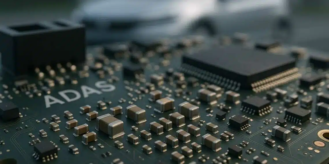
Advanced driver-assistance systems (ADAS) rely heavily on multi-sensor fusion, where radar, LiDAR, ultrasonic sensing, and camera modules continuously exchange high-frequency data. To maintain real-time performance and safety-critical reliability, the ADAS PCB must deliver low-loss signal transmission, stable dielectric behavior, and tight impedance control under prolonged automotive thermal and vibration stress. High-frequency ADAS RF chains—particularly 24...
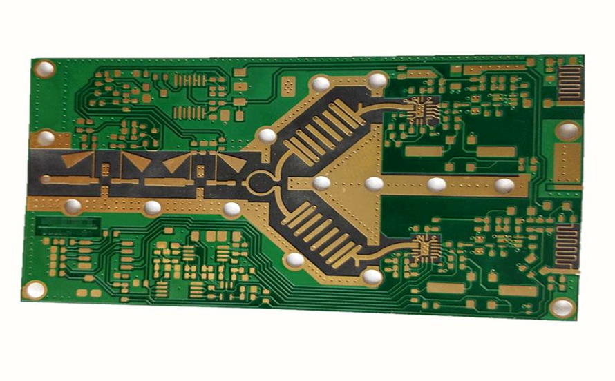
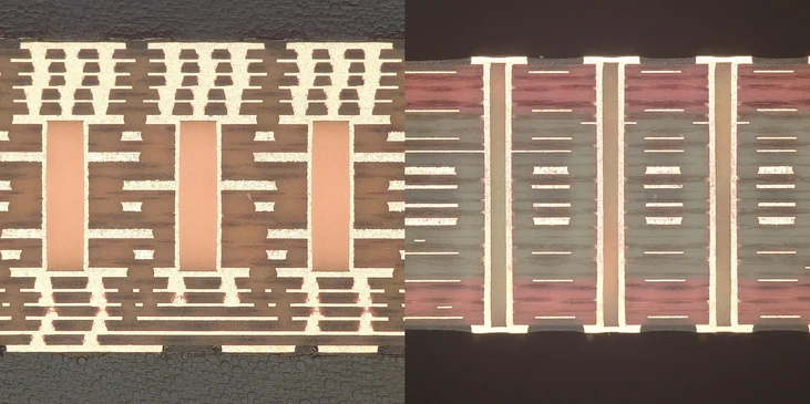
Enhance Thermal Management and Low-Loss Transmission with RO4350B PCB Stackups for 5G mmWave Base Station Units

5G mmWave base station modules require high-frequency RF interconnects that maintain low insertion loss, phase stability, and impedance accuracy under high power and dense component placement. Thermal hotspots and EMI in multilayer architectures can severely degrade link performance and reduce overall throughput. RO4350B PCB laminates (Dk = 3.48 ± 0.02, Df = 0.0037 @10 GHz)...

Maximize RF Channel Integrity and Minimize Signal Loss with Blind Via PCB Architectures for High-Speed Communication Modules

High-speed communication modules in 5G, satellite transceivers, and high-frequency computing systems demand extreme precision in signal routing and interconnect integrity. As layer density increases and modules become more compact, traditional through-hole vias introduce unwanted parasitic effects, signal reflection, and EMI interference, compromising both channel fidelity and system performance. Blind via PCB technology enables selective inter-layer...

Extend High-Temperature RF Reliability and Maintain Ultra-Tight Impedance Stability Using Multilayer HF PCB Architectures for Harsh-Environment IoT Gateways

Harsh-environment IoT gateways—used in industrial automation, outdoor base stations, energy systems, mining networks, and smart transportation infrastructure—operate under extreme thermal stress and wideband RF loading. These platforms demand stable impedance, low-loss transmission, and high-temperature RF reliability to maintain continuous connectivity across Sub-6 GHz, C-Band, and mmWave IoT communication channels. Multilayer HF PCB architectures, built with...

Optimize Signal Integrity and Multi-Band RF Stability with 5G Router PCB Architectures Using Low-Loss Materials

Next-generation 5G routers operate across 2.4, 5, and 6 GHz bands while supporting high-speed MIMO data streams and concurrent RF channels. Maintaining signal integrity, low insertion loss, and impedance accuracy across multilayer PCB architectures is critical for throughput, link stability, and network reliability. Low-loss PCB laminates (Dk ~3.0 ±0.04, Df ~0.0012 @10 GHz) provide minimal...

Enhance Wideband Signal Integrity and Suppress Mode Conversion with Multilayer HF PCB Stackups for Next-Generation RF Sensing Architectures

Next-generation RF sensing architectures, including automotive ADAS radar modules, industrial LiDAR, and high-resolution environmental sensors, demand wideband signal fidelity, minimal mode conversion, and low insertion loss across multilayer PCB interconnects. Phase stability and impedance accuracy are critical to ensure precise beamforming, timing synchronization, and high-speed data acquisition. Multilayer HF PCB laminates with controlled dielectric properties...

Achieve High-Frequency Channel Reliability and Precision Impedance Control with Megtron 7 PCB Stackups in Advanced Server Motherboards

Modern high-performance server motherboards handle multi-gigabit data streams across PCIe Gen5/Gen6, DDR5 memory, and high-speed interconnects. Ensuring channel reliability, minimal signal attenuation, and precise impedance control is critical to maintain data integrity, low bit error rates (BER), and thermal stability in dense server environments. Megtron 7 PCB laminates (Dk = 3.4 ± 0.03, Df =...

Extend Thermal Endurance and RF Power Efficiency with RO4835 PCB Substrates in High-Density Microwave Amplifier Designs

High-density microwave amplifiers, widely used in radar, satellite communication, and 5G mmWave systems, operate under intense thermal stress and high RF power. Maintaining ultra-low insertion loss, precise phase stability, and tight impedance control is critical to ensure amplifier efficiency, signal fidelity, and overall system reliability. RO4835 PCB laminates (Dk = 3.48 ± 0.03, Df =...