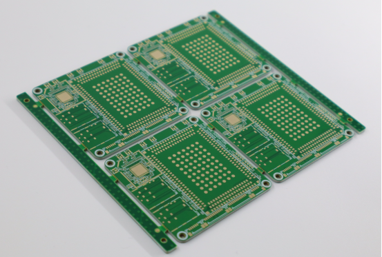
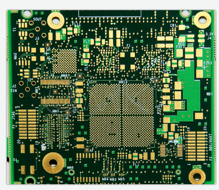
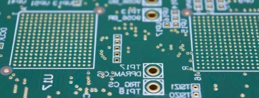
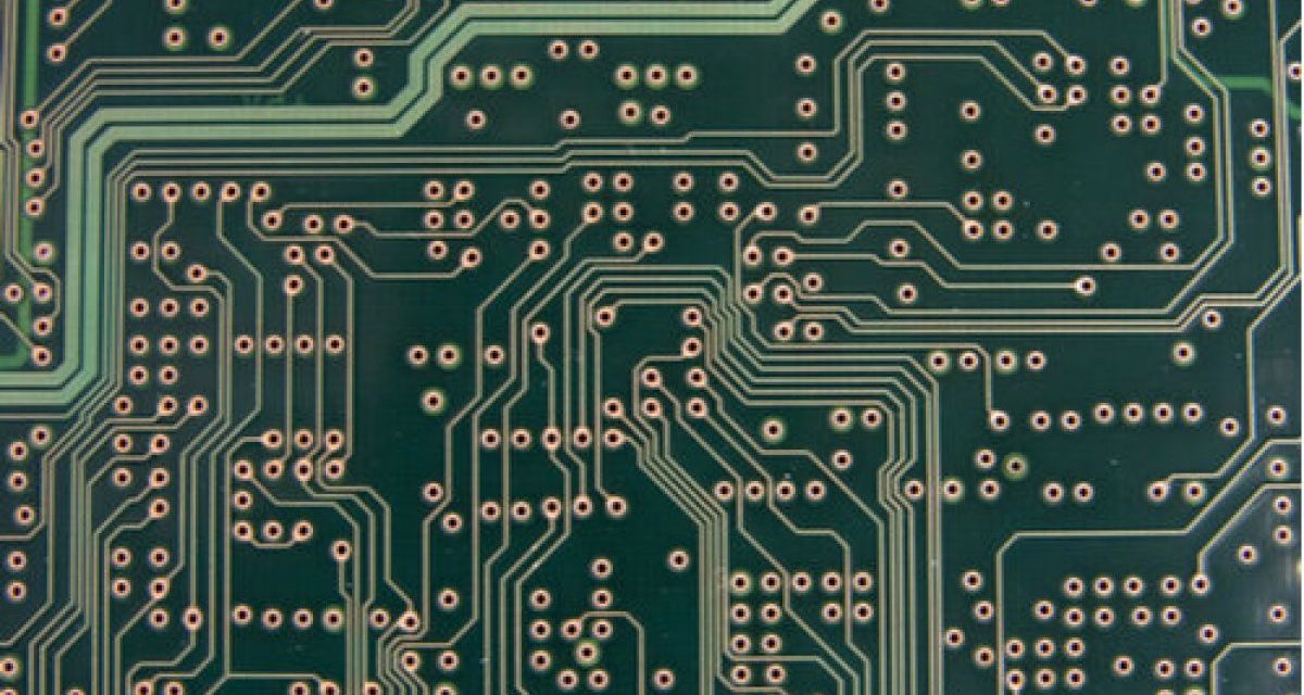
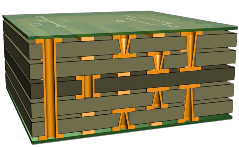
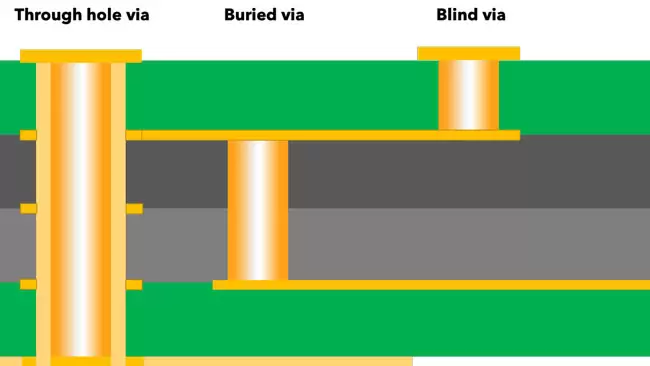
High Density Interconnect PCB - KKPCB
 
HomeTag

High Density Interconnect PCB - KKPCB

Fine Line PCB: High-Density Circuit Design for Advanced Electronics

Fine Line PCB: High-Density Circuit Design for Advanced Electronics As electronic devices continue to become smaller, faster, and more integrated, traditional PCB manufacturing technologies are often insufficient to meet the demands of modern circuit density. Fine Line PCB technology enables the creation of extremely narrow traces and spaces, allowing engineers to design highly compact and...

Microvia PCB Technology: Enabling High-Density Interconnect Designs

As electronic products continue to shrink in size while increasing in functionality, traditional PCB technologies face limitations in routing density and signal performance. Microvia PCB technology has emerged as a key solution for supporting high-density interconnect (HDI) designs in modern electronics. By using extremely small vias to connect circuit layers, microvia PCBs allow engineers to...

HDI PCB: Design, Microvia Technology, and High-Density Applications

High Density Interconnect (HDI) PCB technology is designed to support modern electronic devices that demand higher performance, smaller form factors, and greater circuit complexity. HDI PCBs use advanced manufacturing techniques such as microvias, blind vias, buried vias, and fine line routing to increase the wiring density compared to traditional multilayer PCBs. As electronic products continue...

HDI PCB – High Density Interconnect PCB for Advanced Electronic Applications

What Is an HDI PCB? An HDI PCB (High Density Interconnect PCB) is a printed circuit board designed with higher wiring density per unit area compared to traditional PCBs. It typically incorporates microvias, blind and buried vias, fine trace widths, and advanced multilayer stack-ups to support compact and high-performance electronic designs. HDI technology enables smaller...

Blind Via PCB – High Density Interconnect PCB for Compact and High Speed Designs

What Is a Blind Via PCB? A Blind Via PCB is a type of printed circuit board that contains vias connecting internal layers to one or more outer layers without passing completely through the board. Unlike through-hole vias, blind vias help: Reduce board size Increase routing density Optimize multilayer stack-ups Support HDI (High Density Interconnect)...

High Density PCB Manufacturing for Advanced Electronic Applications

What Is a High Density PCB? A High Density PCB (High Density Printed Circuit Board) is designed to accommodate more components, higher pin counts, and finer routing within a limited board area. It is widely used in applications that require compact size, high performance, and complex signal routing, such as semiconductor testing, telecommunications, automotive electronics,...

HDI PCB: High Density Interconnect PCB Manufacturing for Advanced Electronic Applications

An HDI PCB (High Density Interconnect PCB) is a key technology enabling compact, lightweight, and high-performance electronic products. As electronic devices continue to evolve toward smaller form factors, higher functionality, and faster data transmission, traditional PCB designs can no longer meet density and routing requirements. HDI PCB technology provides higher wiring density per unit area...

Buried Via PCB for High-Density and Advanced Multilayer Circuit Designs

What Is a Buried Via PCB? A Buried Via PCB is a multilayer printed circuit board that uses vias connecting only internal layers without reaching the outer surface layers. These hidden interconnections allow designers to increase routing density while maintaining surface space for components and signal traces. Buried Via PCBs are widely used in HDI...

Microvia PCB: Advanced HDI PCB Technology for Miniaturized and High-Performance Electronics

Introduction to Microvia PCB A Microvia PCB is a key enabling technology in HDI (High Density Interconnect) PCB manufacturing, designed to meet the increasing demands for miniaturization, high-speed signal transmission, and high component density. By using laser-drilled microvias, Microvia PCBs significantly reduce interconnect length, improve routing flexibility, and enhance overall electrical performance. Microvia PCB technology...

HDI PCB: High-Density Interconnect Technology for Compact and High-Speed Electronic Designs

As electronic products continue to evolve toward smaller form factors and higher performance, conventional PCB technologies often reach their limits. The HDI PCB (High-Density Interconnect PCB) overcomes these limitations by enabling ultra-dense routing, shorter signal paths, and enhanced electrical performance. A professionally engineered HDI PCB is essential for modern high-speed and high-density electronic systems. What...