Controlled Impedance PCB - KKPCB
 
HomeTag

Controlled Impedance PCB - KKPCB

ATE PCB Prototype: Fast and Reliable Platforms for Test System Validation

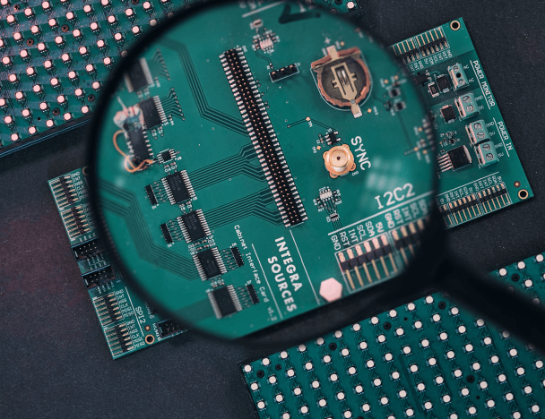
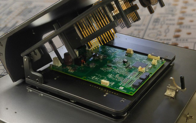
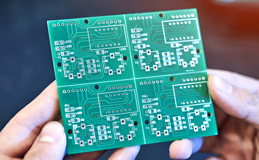
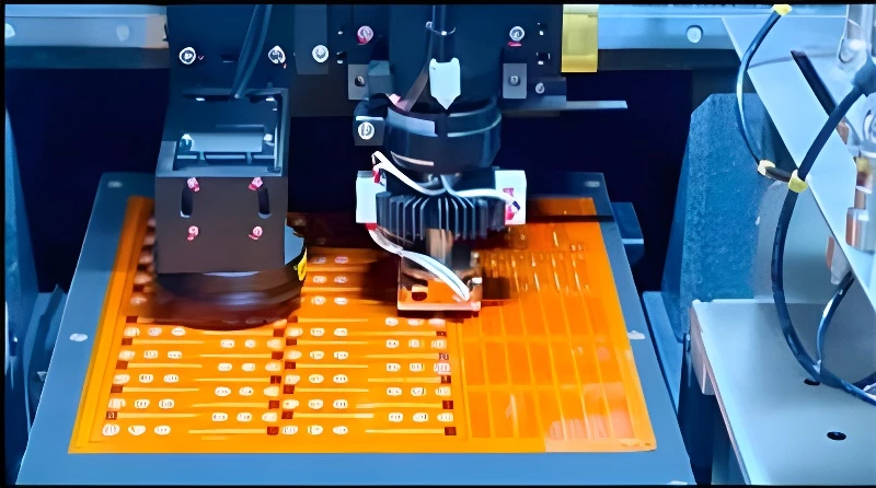
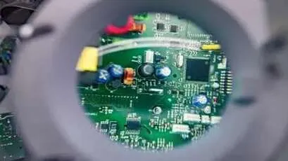
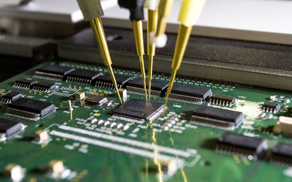
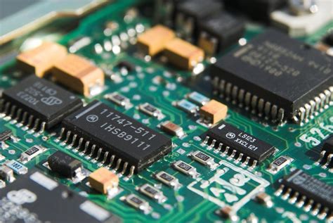
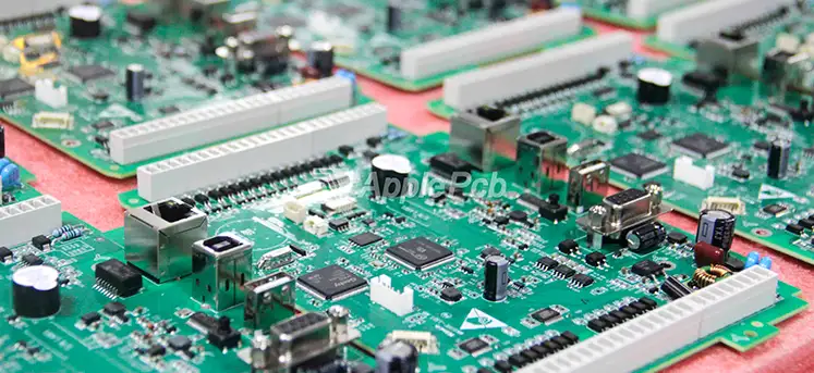
In automated test equipment development, early-stage validation determines long-term system reliability. The ATE PCB Prototype provides a controlled platform for verifying electrical performance, mechanical interfaces, and test repeatability before production deployment. A well-designed ATE PCB prototype reduces risk and accelerates development cycles. Role of ATE PCB Prototypes in Test Engineering An ATE PCB Prototype bridges...

High Speed Test PCB: Precision Platforms for High-Speed Signal Validation and Test Accuracy

As data rates continue to increase across modern electronics, validating high-speed signals becomes more challenging. The High Speed Test PCB provides a stable and repeatable platform for evaluating signal integrity, timing, and performance in high-speed digital and mixed-signal systems. High speed test PCBs are essential for accurate measurement and debugging. What Is a High Speed...

Custom Probe Card PCB: Precision PCBs for Advanced Wafer-Level Semiconductor Testing

As semiconductor devices move toward higher speed, finer pitch, and greater integration, wafer-level testing demands extreme precision. The Custom Probe Card PCB forms the electrical backbone of probe card assemblies, enabling accurate signal transmission between automated test equipment and devices under test (DUTs) on the wafer. A well-designed custom probe card PCB directly impacts test...

Semiconductor Testing PCB: High-Reliability PCBs for Advanced Device Validation and Production Testing

As semiconductor devices continue to scale in speed, complexity, and pin count, testing accuracy becomes critical. The Semiconductor Testing PCB serves as the core platform connecting devices under test (DUTs) with automated test equipment (ATE), enabling precise electrical characterization and reliable production testing. High-quality semiconductor testing PCBs are essential for yield improvement and risk reduction....

High Layer Count ATE PCB: Advanced Multilayer Platforms for High-Density Test Systems

As automated test equipment evolves to support faster data rates and higher pin counts, PCB complexity increases significantly. The High Layer Count ATE PCB provides the routing density, power integrity, and signal control required for modern semiconductor testing. High layer count designs are essential for advanced ATE performance and scalability. What Is a High Layer...

Rigid-Flex Test PCB: Space-Efficient and Reliable Solutions for Advanced Test Applications

As test systems become more compact and complex, traditional rigid PCBs often struggle to meet mechanical and routing constraints. The Rigid-Flex Test PCB combines rigid board stability with flexible interconnections, enabling reliable testing in space-limited and mechanically dynamic environments. Rigid-flex technology is increasingly essential for modern test and validation platforms. What Is a Rigid-Flex Test...

Small Batch ATE PCB: Reliable Low-Volume Manufacturing for Test Engineering and NPI

Between initial prototyping and full-scale production, test engineers often require a controlled, repeatable manufacturing stage. Small batch ATE PCB production fills this gap by providing consistent quality, stable electrical performance, and scalable processes for automated test equipment (ATE) development. Small batch manufacturing enables engineering teams to validate real production conditions without the risks of mass...

ATE PCB Prototype: Rapid Validation Platforms for Automated Test Equipment Development

Before an automated test system enters production, its electrical and mechanical behavior must be thoroughly validated. The ATE PCB Prototype serves as the critical platform for early-stage verification, allowing engineers to evaluate signal integrity, power delivery, and interface compatibility under real test conditions. A well-executed ATE PCB prototype reduces development risk and accelerates time to...

High Speed Test PCB: Signal Integrity and Timing Accuracy for High-Speed Digital Validation

As data rates continue to increase, validating high-speed digital interfaces requires test platforms that introduce minimal distortion. The High Speed Test PCB is engineered to act as a transparent signal medium, enabling accurate characterization of high-speed devices and systems. A well-designed high speed test PCB ensures that test results reflect real device performance rather than...

Probe Card PCB Assembly: Precision Assembly for Reliable Wafer-Level Semiconductor Testing

In wafer-level semiconductor testing, even microscopic assembly deviations can lead to unstable probe contact and inconsistent measurements. Probe Card PCB Assembly is a highly specialized process that integrates probe structures, connectors, and high-density routing into a mechanically and electrically stable test platform. A professionally executed probe card PCB assembly directly determines test accuracy, probe lifetime,...