Compact PCB Design - KKPCB
 
HomeTag

Compact PCB Design - KKPCB

Rigid-Flex PCBs: Combining Rigidity and Flexibility for Advanced Electronics

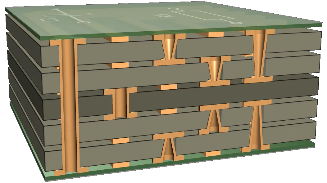
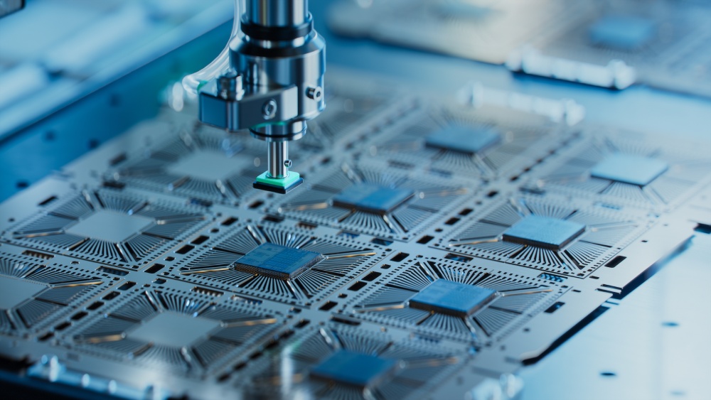
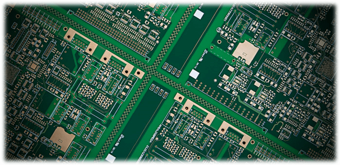
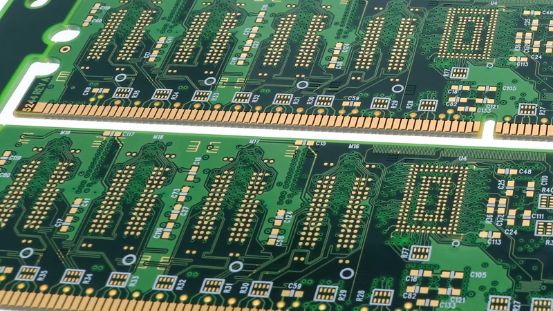
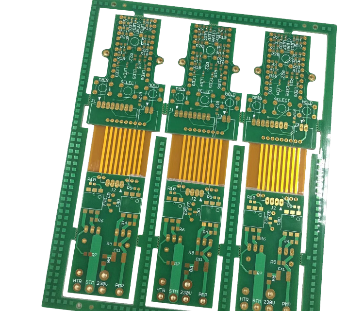
A Rigid-Flex PCB is a printed circuit board that combines rigid sections with flexible circuits into a single, integrated assembly. This design enables 3D packaging, reduced interconnects, and improved reliability in applications where traditional rigid PCBs cannot meet space or mechanical constraints. Rigid-Flex technology is essential in: Aerospace and defense electronics Medical devices Industrial automation...

Blind Via PCBs: High-Density Interconnections for Advanced Electronics

A Blind Via PCB is a multilayer printed circuit board that uses vias connecting an outer layer to one or more inner layers without extending through the entire board. Unlike through-hole vias, blind vias do not penetrate all layers, allowing for high-density routing, reduced board size, and improved signal integrity. Blind via technology is critical...

Buried Via PCB – Advanced Multilayer PCB Technology for High-Density Circuit Design

What Is a Buried Via PCB? A Buried Via PCB is a type of multilayer printed circuit board that uses buried vias to connect internal copper layers without reaching the outer surface layers. Unlike through-hole vias that pass through the entire board, buried vias exist only between inner layers, remaining invisible from the exterior of...

HDI PCB – High Density Interconnect PCB for Advanced Electronics

What Is HDI PCB? HDI PCB (High Density Interconnect PCB) is a printed circuit board designed with higher wiring density per unit area compared to traditional multilayer PCBs. It uses advanced manufacturing technologies such as microvias, blind vias, buried vias, and fine line traces to achieve compact size and improved electrical performance. HDI PCB is...

Buried Via PCB – Advanced Multilayer PCB with Internal Interconnection Technology

What Is a Buried Via PCB? A Buried Via PCB is a multilayer printed circuit board that contains vias connecting internal layers only, without reaching the outer surface layers. Unlike through-hole vias, buried vias are completely enclosed within the board stack-up. This allows designers to: Increase routing density Optimize outer layer space Improve signal integrity...

Fine Pitch PCB: Precision Manufacturing for High Pin Count and Miniaturized Electronics

A Fine Pitch PCB is a printed circuit board specifically designed to support high pin count ICs and ultra-small component spacing, commonly found in modern semiconductor devices, high-speed electronics, IoT modules, automotive electronics, and advanced test boards. As electronic products continue to shrink while integrating more functions, fine pitch PCB technology has become essential for...

High Density PCB: Advanced Design and Manufacturing for Compact and High-Performance Electronics

A High Density PCB (HDPCB) is a specialized printed circuit board designed for compact, high-performance, and high-pin-count electronic applications. HD PCBs are widely used in semiconductor test boards, IoT devices, wearable electronics, automotive systems, and high-speed communication modules, where space constraints, signal integrity, and reliability are critical. High density PCBs combine fine-pitch component layouts, multilayer...

High Density PCB: Advanced PCB Solutions for Compact and High-Performance Electronics

A High Density PCB is a specialized printed circuit board designed to support compact layouts, high pin count components, and complex signal routing within limited space. As electronic devices continue to shrink while increasing in performance, high density PCB technology has become essential for applications requiring high-speed data transmission, high-frequency signals, and reliable power delivery....