PCB Design Services | Professional PCB Layout & Design - KKPCB
 
HomeCategory

PCB Design Services | Professional PCB Layout & Design - KKPCB

PCB Routing: Best Practices for Ensuring Signal Integrity and Performance

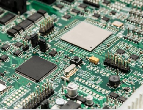
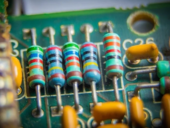
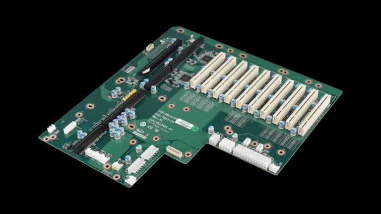
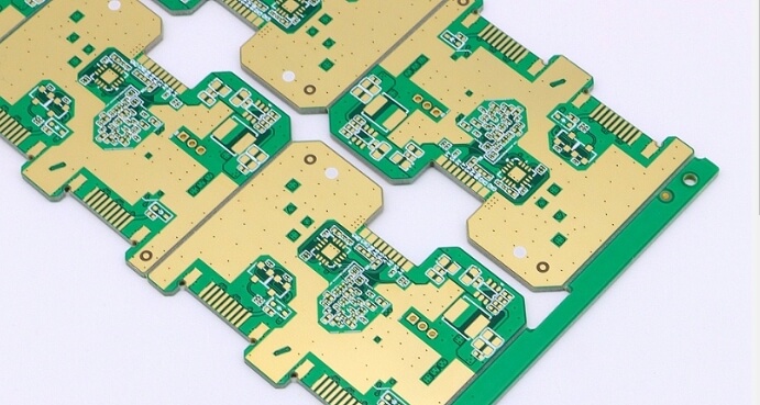
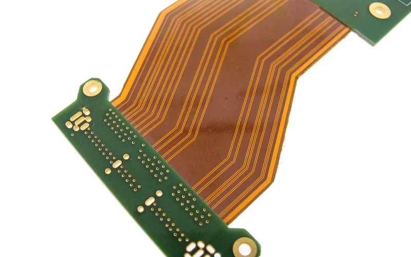
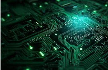
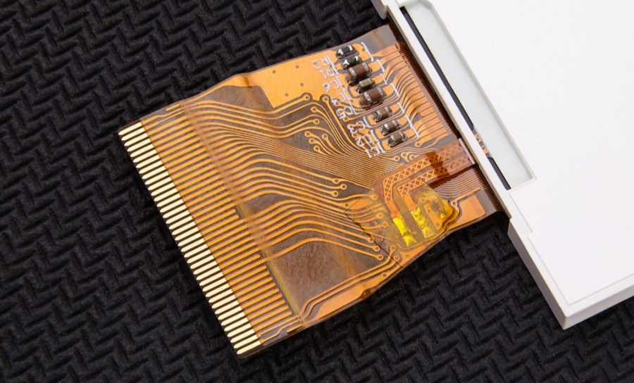
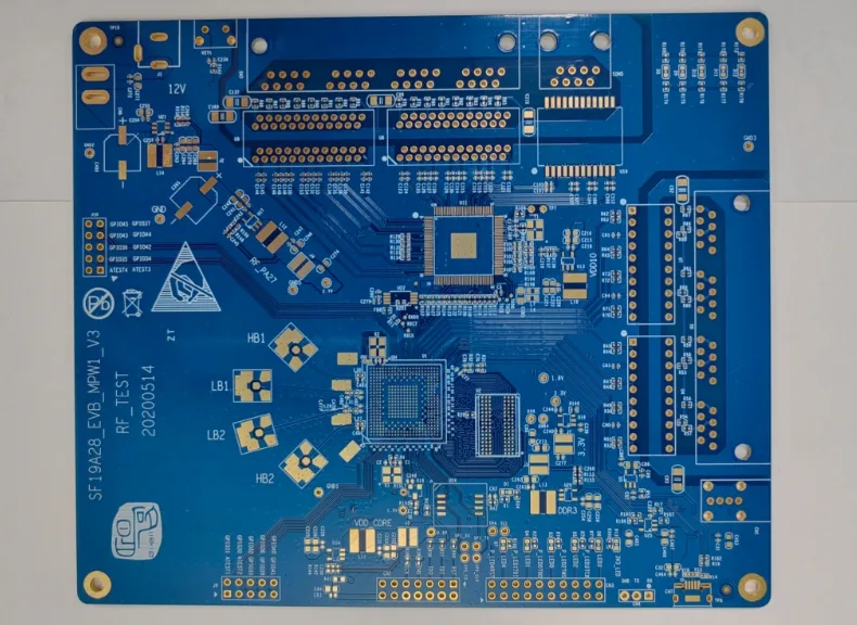
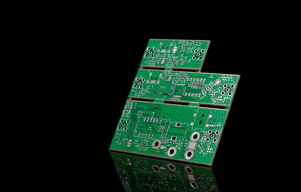
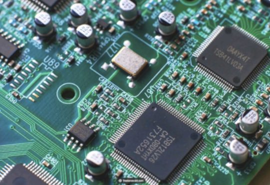
Printed Circuit Board (PCB) routing is a critical aspect of electronic design, ensuring that electrical signals are transmitted efficiently and reliably between components. Proper routing minimizes interference, maintains signal integrity, and meets design requirements such as impedance control and thermal management. This article outlines the best practices for PCB routing, focusing on optimizing performance and ensuring signal integrity....

PCB Thermal Design Guide: Tips For PCB Analysis and Performance

Electronics are becoming faster, smaller, and used in more demanding environments. Miniaturized ICs and SMDs operate at higher frequencies and require more power. Increased current demands cause voltage drops across resistive elements, generating heat and leading to temperature rises and hotspots. Over half of electronic component failures now stem from heat-related stress. To develop high-quality circuit...

PCB Resistors and Board Design

PCB resistors are designed to be mounted and soldered to printed circuit boards; they control current flow and divide voltages, among other things.  PCB resistors come in many shapes and sizes, but they’re all designed to fit easily into board layouts. They have two terminals that can be soldered to the conductive traces on the PCB so they...

KKPCB Case Study: High-Performance Communication Backplane PCB Solution

Introduction: Enabling High-Speed Communication Systems In today’s data-driven world, high-speed communication systems demand exceptional signal integrity, power stability, and system reliability. At the core of these systems lies the communication backplane PCB, which serves as the backbone for high-speed data transmission between multiple modules. This case study highlights how KKPCB delivered a high-performance backplane PCB...

Grounding method in multilayer PCB circuit board

In modern multilayer PCB circuit board design, selecting the correct grounding method is essential for ensuring optimal signal integrity, minimizing electromagnetic interference (EMI), and maintaining stable power integrity. A well-designed grounding system not only improves overall PCB performance but also enhances the reliability of high-speed and high-frequency electronic applications. One of the most widely used...

Why You Need Rigid Circuit Boards from KKPCB

In modern electronics manufacturing, rigid circuit boards are the foundation of reliability, stability, and performance. From industrial automation to consumer electronics, Rigid PCBs are widely used due to their durability and cost efficiency. When it comes to sourcing high-quality rigid circuit boards, KKPCB is a trusted partner delivering precision, consistency, and scalability. What Are Rigid...

About PCB Layer Stackup

A PCB Layer Stackup refers to the arrangement of conductive copper layers and insulating dielectric materials that make up a multilayer PCB. In the era of high-speed digital electronics and 5G, the stackup is no longer just a mechanical carrier; it is a critical tool for managing signal integrity, power distribution, and electromagnetic compatibility (EMC). A well-engineered stackup from KKPCB ensures...

What is the difference between flexible PCB and just scratching the printing circuit board?

1. What Is a Flexible PCB? A flexible PCB (Flex PCB) is a specially engineered printed circuit board made from flexible materials such as polyimide. It is designed to bend, twist, or fold without damaging the circuit. Key Characteristics: Built on flexible substrates (e.g., polyimide) Designed for dynamic or static bending High reliability under mechanical...

PCB Prototyping Services

In modern electronics development, PCB prototyping services play a critical role in transforming circuit concepts into functional hardware. Whether for high-speed PCB design, RF PCB development, or industrial electronics, fast and accurate PCB prototype manufacturing ensures design validation, reduces risks, and accelerates time-to-market. Professional PCB prototyping services provide engineers with rapid turnaround, high-quality fabrication, and...

Blind Via and Buried Via

In modern PCB design, Blind Via and Buried Via technologies play a critical role in achieving high-density interconnect (HDI) structures, improving signal integrity, and optimizing PCB layout performance. As electronic devices continue to evolve toward miniaturization, high speed, and high functionality, the use of blind vias and buried vias has become increasingly essential in advanced...