kkpcb04 - KKPCB - Page 65 of 104
 
HomeAuthor

kkpcb04 - KKPCB - Page 65 of 104

ODM PCB Services: Integrated Design, Prototyping, and Manufacturing Solutions

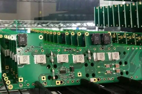
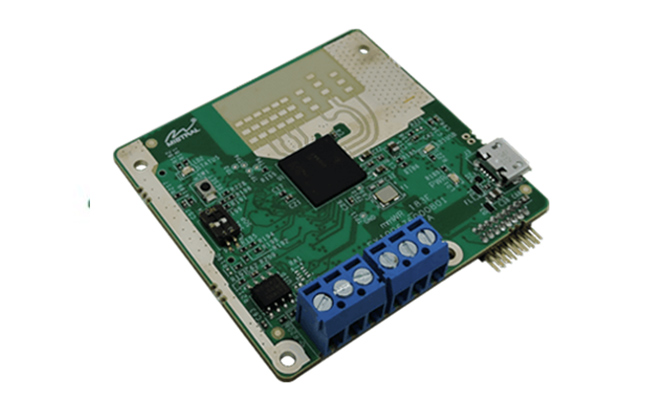
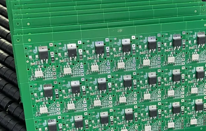
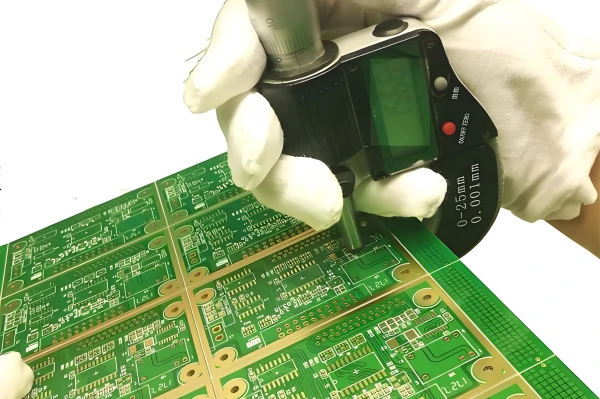
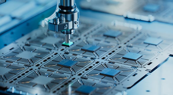
In an increasingly competitive electronics market, shortening development cycles while maintaining product quality has become a major challenge for OEMs and system developers. ODM PCB services address this challenge by integrating PCB design, engineering validation, fabrication, and assembly into a single, efficient workflow. By working with an experienced ODM PCB partner, companies can reduce coordination...

Fast Delivery PCB: Accelerating Product Development with Rapid PCB Manufacturing

In today’s highly competitive electronics market, speed is often the key differentiator between success and missed opportunity. Fast delivery PCB services enable engineers, startups, and OEMs to shorten development cycles, validate designs faster, and respond quickly to market demands. Whether for early-stage prototypes, small-batch production, or urgent engineering revisions, fast delivery PCB manufacturing plays a...

Memory Test PCB: High-Precision Solutions for DRAM, SRAM, and Flash Testing

As memory devices become faster and more complex, Memory Test PCBs play a critical role in ensuring IC reliability, signal integrity, and yield. These specialized PCBs serve as the interface between memory chips and automated test equipment (ATE), providing precise routing, high pin count support, and controlled impedance for accurate testing. From wafer-level validation to...

Chip Test PCB: Precision Testing Solutions for Advanced Semiconductor Devices

As semiconductor devices continue to scale in speed, density, and complexity, chip-level testing has become essential for ensuring product quality, yield, and reliability. Chip Test PCBs act as the interface between the chip under test and automated test equipment (ATE), providing precise signal routing, controlled impedance, and high-density connections for accurate semiconductor validation. High-quality chip...

Wafer Test PCB for High-Precision Semiconductor and ATE Applications

In modern semiconductor manufacturing, wafer-level testing is a critical step to ensure IC functionality, yield, and quality before packaging. Wafer Test PCBs serve as the electrical interface between probe cards and automated test equipment (ATE), enabling accurate signal transmission, high-density connections, and controlled impedance for reliable testing of wafers. By using high-quality wafer test PCBs,...

IC Testing PCB Solutions for Accurate and Reliable Semiconductor Validation

As semiconductor devices continue to scale in speed, density, and complexity, IC testing PCB has become a critical component in ensuring chip performance, reliability, and yield. From wafer-level testing to final package validation, IC testing PCBs act as the electrical interface between the device under test (DUT) and automated test equipment (ATE). High-quality IC testing...

ODM PCB: Integrated Design and Manufacturing Solutions for Custom Electronics

In today’s fast-evolving electronics market, speed, reliability, and manufacturability are just as critical as innovation. ODM PCB services bridge the gap between product concept and mass production by offering a fully integrated workflow that combines engineering design, PCB fabrication, and assembly under one roof. Rather than managing multiple vendors for design, prototyping, and production, companies...

Fast Delivery PCB: Rapid Prototyping and Small-Batch Solutions for High-Performance Electronics

In today’s fast-paced electronics and semiconductor industry, speed and reliability are critical. Engineers often need to validate designs quickly, iterate rapidly, and move from prototypes to production with minimal delay. Fast delivery PCBs provide the ideal solution by offering rapid prototyping, small-batch manufacturing, and high-quality boards that meet strict electrical and mechanical requirements. These PCBs...

Semiconductor Testing PCB: Reliable Solutions for High-Precision IC Validation

In the era of advanced semiconductor devices, accurate testing is critical for ensuring product quality and yield. Semiconductor Testing PCBs are specialized printed circuit boards designed to interface between integrated circuits (ICs) and automated test equipment (ATE), providing precise electrical connections, controlled impedance, and robust mechanical support. These PCBs are fundamental to wafer-level testing, IC...

High Layer Count ATE PCB: Advanced Multilayer Solutions for Semiconductor Test

As semiconductor devices become more complex with increasing pin counts and high-speed signal requirements, high layer count ATE PCBs have become essential for accurate automated test equipment (ATE) operation. These multilayer boards enable dense routing, controlled impedance, and reliable signal integrity, ensuring precise and repeatable semiconductor testing. High layer count ATE PCBs allow engineers to...