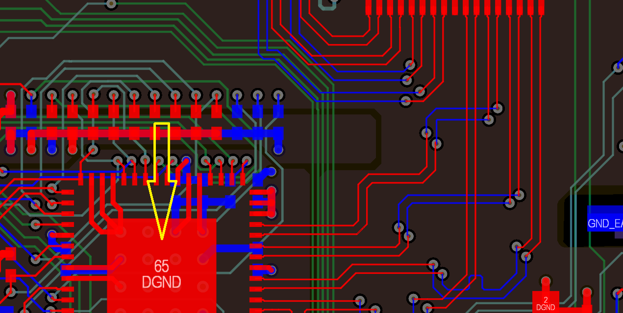
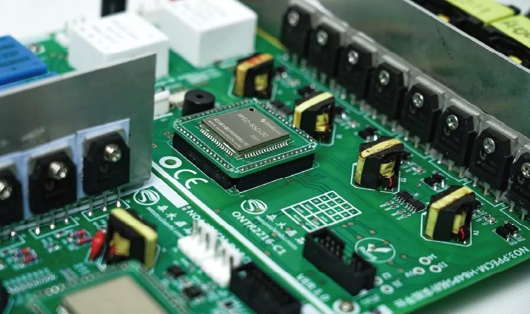
signal integrity PCB - KKPCB
 
HomeTag

signal integrity PCB - KKPCB

HDI PCBs: High-Density Interconnect Solutions for Next-Generation Electronics

Why HDI PCBs Are No Longer Optional As electronic devices become smaller, faster, and more complex, traditional multilayer PCB designs struggle to keep up. HDI (High-Density Interconnect) PCBs address this challenge by enabling higher routing density, shorter signal paths, and better electrical performance. At the core of HDI technology is the use of: Microvias (laser-drilled...

High Pin Count PCBs: Enabling Complex Interconnections in Advanced Electronics

Why High Pin Count Matters As modern electronic systems evolve, integrated circuits such as CPUs, GPUs, FPGAs, and high-speed SoCs demand hundreds or even thousands of I/O connections. A High Pin Count PCB is designed to support these devices by enabling dense interconnections within limited board space. Unlike standard PCB designs, high pin count boards...

5G mmWave PCBs: Engineering for Ultra-High Frequency Performance

Why mmWave Changes Everything The transition from sub-6 GHz to millimeter wave (mmWave) frequencies fundamentally changes PCB design. Operating typically between 24 GHz and 100 GHz+, mmWave systems push PCB technology to its limits. At these frequencies, the PCB is no longer just a passive interconnect—it becomes an active part of the RF system, directly...

Load Board PCBs: Critical Interfaces for Accurate Semiconductor Testing

Role in Test System A Load Board PCB serves as the primary electrical interface between Automated Test Equipment (ATE) and the Device Under Test (DUT). While probe cards operate at the wafer level, load boards are typically used in package-level testing, where ICs are already packaged and mounted into sockets. In a typical test setup,...

Probe Card PCBs: Precision Platforms for Semiconductor Testing

What Makes Probe Card PCBs Unique A Probe Card PCB is not a typical circuit board—it is a high-precision interface platform used in semiconductor wafer testing. It connects test equipment (ATE) to microscopic pads on silicon wafers through probe needles or MEMS structures. Unlike standard PCBs, probe card boards must support: Ultra-fine pitch interconnections High...

Buried Via PCBs: Strategic Layer Interconnects for High-Performance Designs

Why Buried Vias Matter As electronic systems become more compact and performance-driven, traditional via structures are no longer sufficient for complex routing requirements. A Buried Via PCB enables connections only between internal layers, eliminating unnecessary vertical paths through the entire board. This design approach is not just about saving space—it is about engineering control over...

High Layer Count PCBs: Advanced Solutions for Complex Electronic Systems

A High Layer Count PCB is a printed circuit board with 8 or more signal layers, often extending to 20–40 layers or more in advanced systems. These boards enable dense routing, compact design, and integration of multiple high-speed and RF circuits in a single assembly. High layer count PCBs are critical in: High-performance computing Networking...

Rigid-Flex PCBs: Combining Rigidity and Flexibility for Advanced Electronics

A Rigid-Flex PCB is a printed circuit board that combines rigid sections with flexible circuits into a single, integrated assembly. This design enables 3D packaging, reduced interconnects, and improved reliability in applications where traditional rigid PCBs cannot meet space or mechanical constraints. Rigid-Flex technology is essential in: Aerospace and defense electronics Medical devices Industrial automation...

Blind Via PCBs: High-Density Interconnections for Advanced Electronics

A Blind Via PCB is a multilayer printed circuit board that uses vias connecting an outer layer to one or more inner layers without extending through the entire board. Unlike through-hole vias, blind vias do not penetrate all layers, allowing for high-density routing, reduced board size, and improved signal integrity. Blind via technology is critical...

Multilayer HF PCBs: Optimized Solutions for High-Frequency, High-Density Designs

A Multilayer HF PCB is a printed circuit board engineered for high-frequency signal transmission across multiple layers. Unlike standard multilayer boards, HF (high-frequency) PCBs are optimized for low dielectric loss, controlled impedance, and minimal crosstalk, enabling high-speed signal integrity in demanding applications. Multilayer HF PCBs are commonly used in: RF and microwave modules Wireless communication...