server PCB – KKPCB
 
HomeTag

server PCB

Buried Via PCB: Advanced Multilayer Interconnects for High-Density Electronics

As electronic devices become smaller and more complex, the need for high-density interconnections within printed circuit boards increases. Buried via PCBs offer a solution by connecting inner layers without using surface space, allowing for compact, high-performance multilayer boards. Buried vias improve routing flexibility, signal integrity, and design density, making them critical for advanced applications such...
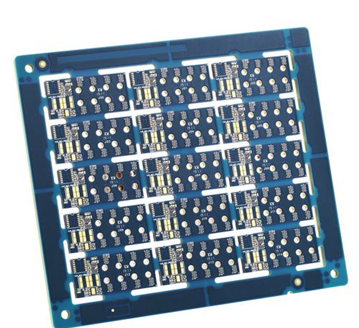
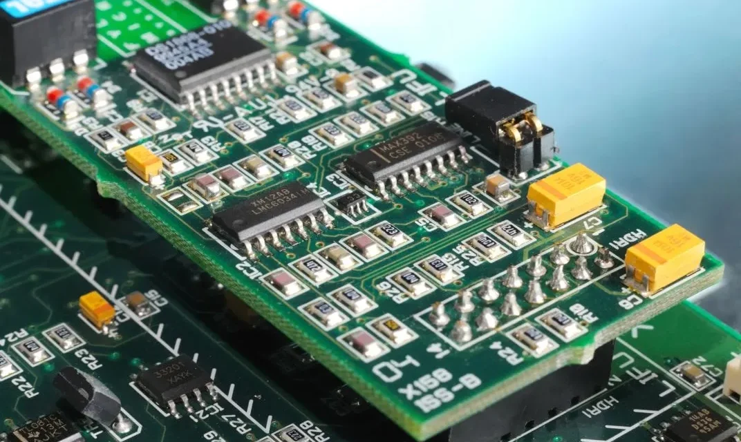
High Layer Count PCB – Advanced Multilayer Boards for Complex Electronic Systems

What Is a High Layer Count PCB? A High Layer Count PCB is a multilayer printed circuit board that contains a large number of conductive layers, typically 12 layers or more, designed to support highly complex electronic systems. These PCBs allow engineers to route dense circuitry while maintaining signal integrity, power stability, and electromagnetic compatibility....

Buried Via PCB – High Density Multilayer PCB with Internal Via Interconnection

What Is a Buried Via PCB? A Buried Via PCB is a multilayer printed circuit board that uses vias connecting only internal layers, without extending to the outer surface layers. Unlike through-hole vias that pass through the entire board thickness, buried vias are fully embedded within the PCB stack-up. This structure improves routing density, reduces...

High Speed PCB – Precision Design for Signal Integrity and High Data Rate Applications

High Speed PCB for Modern Digital Systems As data rates continue to increase in communication, computing, and semiconductor applications, PCB design must evolve to maintain signal integrity and stable performance. A High Speed PCB is specifically engineered to support high-frequency digital signals, fast edge rates, and high bandwidth transmission. Unlike standard PCBs, high speed boards...

Controlled Impedance PCB – High Speed PCB for Reliable Signal Transmission

What Is a Controlled Impedance PCB? A Controlled Impedance PCB is a printed circuit board engineered to maintain a precise and consistent impedance value along specific signal traces. Impedance control is critical in high speed and high frequency electronic systems where signal integrity directly affects performance and reliability. In modern electronic designs, signals travel at...

Buried Via PCB – Advanced Multilayer PCB with Internal Interconnection Technology

What Is a Buried Via PCB? A Buried Via PCB is a multilayer printed circuit board that contains vias connecting internal layers only, without reaching the outer surface layers. Unlike through-hole vias, buried vias are completely enclosed within the board stack-up. This allows designers to: Increase routing density Optimize outer layer space Improve signal integrity...

High Layer Count PCB – Advanced Multilayer PCB for High Density and High Speed Applications

What Is a High Layer Count PCB? A High Layer Count PCB refers to a multilayer printed circuit board typically built with 16 layers or more, and in advanced applications, up to 40, 60, or even higher layer counts. High Layer Count PCB is designed to support: High density routing Complex signal distribution Controlled impedance...

High TG PCB – High Glass Transition Temperature PCB for High Reliability Applications

What Is a High TG PCB? A High TG PCB is a printed circuit board fabricated using high glass transition temperature (TG) laminate materials, typically with TG values above 170°C, 180°C, or even 200°C depending on application requirements. The glass transition temperature (TG) refers to the temperature at which the PCB substrate transitions from a...

Megtron PCB Manufacturing Guide: Benefits, Applications & Material Options

Megtron PCB: A Low-Loss Solution for High-Speed Digital and Advanced Electronics As electronics continue to evolve toward higher data rates, lower latency, and greater integration, PCB materials play a critical role in maintaining signal quality. In high-speed applications such as data centers, servers, 5G infrastructure, and high-performance networking equipment, signal loss and impedance instability can...

Megtron PCB: Low-Loss High-Speed Material for Signal Integrity and High-Frequency Applications

As electronic systems continue to deliver higher bandwidth, faster data rates, and more compact designs, PCB material selection becomes a key factor in achieving stable and reliable performance. In high-speed digital systems and high-frequency applications, traditional FR-4 materials may cause excessive signal loss, impedance instability, and increased crosstalk, especially when signals operate at multi-GHz frequencies....