RF Trace Design - KKPCB
 
HomeTag

RF Trace Design - KKPCB

RF Trace PCB Design: Optimizing High-Frequency Signal Paths for Maximum Performance

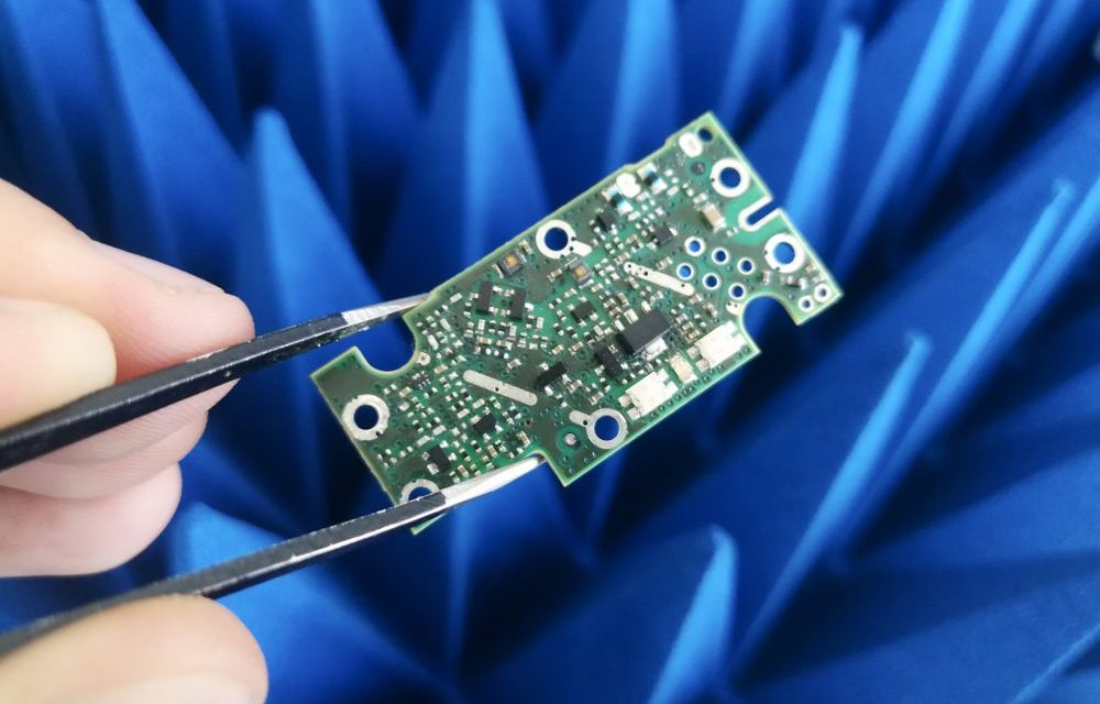
What Is an RF Trace PCB? An RF Trace PCB is a specialized RF PCB where signal routing is designed as controlled transmission lines to carry high-frequency signals with minimal loss and distortion. In RF Trace PCB design, traces are no longer simple connections—they function as engineered RF signal paths, where geometry, materials, and layout...

RF Trace PCB: Precision RF Routing for Low-Loss and Stable High-Frequency Signal Transmission

As wireless technologies continue to evolve toward higher frequencies and greater bandwidth, RF performance requirements have become more demanding than ever. From 5G communication and WiFi 6/6E to GPS, radar, and microwave RF modules, the quality of RF routing on the PCB directly impacts signal stability, insertion loss, and overall system reliability. An RF Trace...