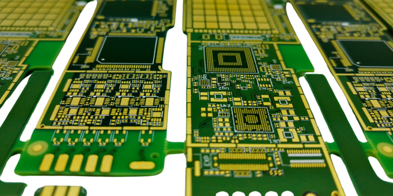
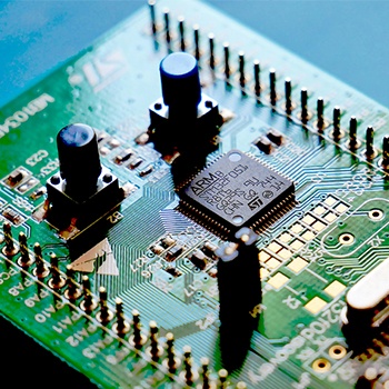
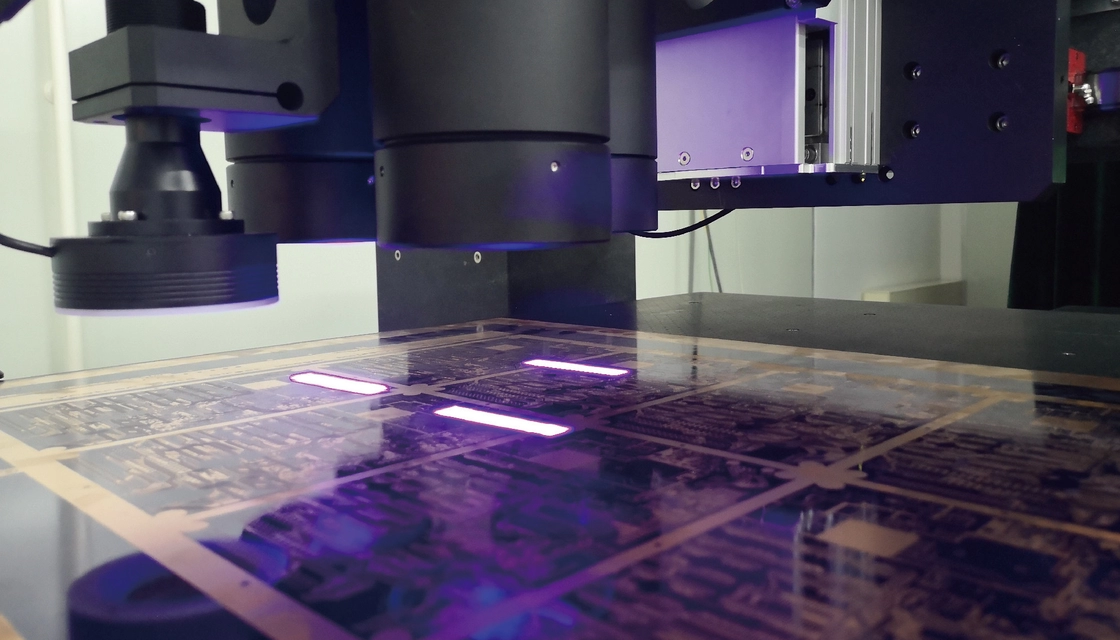
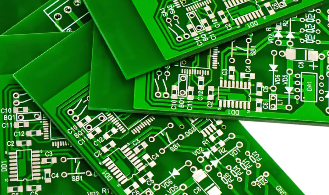
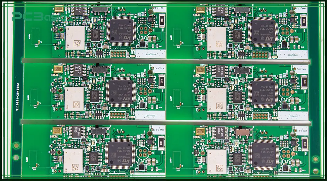
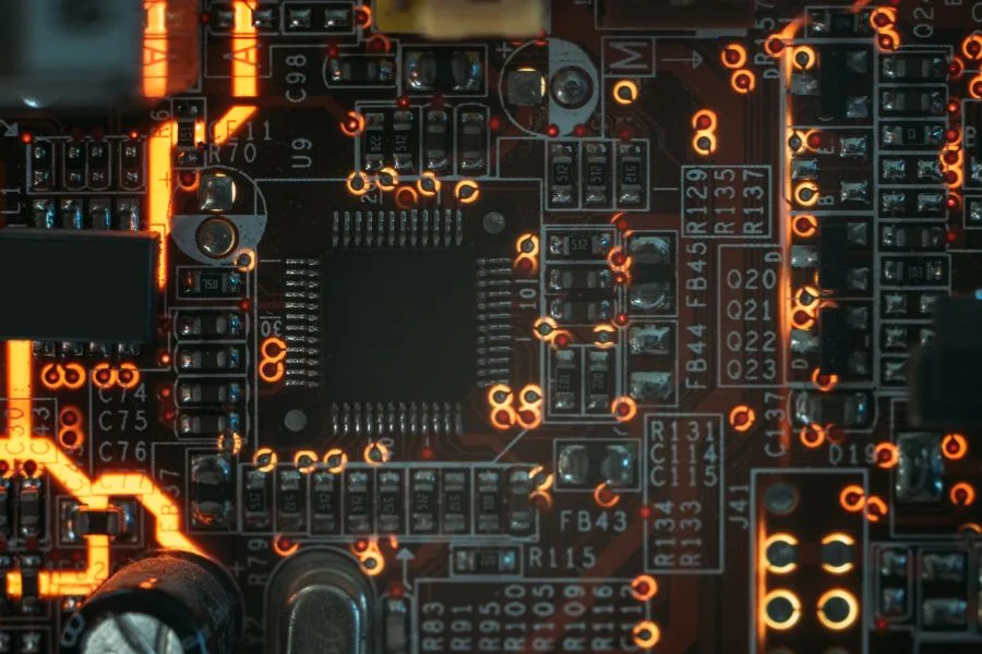
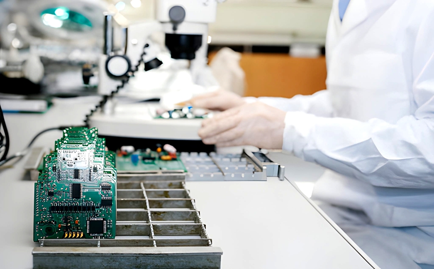
PCB manufacturing - KKPCB
 
HomeTag

PCB manufacturing - KKPCB

Control of Conductor Etching in PCB Manufacturing: Precision Copper Etching for Fine-Line Circuit Patterns

Control of Conductor Etching Process in Printed Circuit Boards Copper etching is one of the most critical steps in printed circuit board (PCB) manufacturing, as it directly determines the accuracy and reliability of conductive circuit patterns. The term “printed circuit board” originates from this process, since etching is the final stage of photolithography used to...

Achieve Low-Loss Transmission and Stable Impedance Performance with Double Layer HF PCB Engineering for High-Frequency Communication Systems

A Double Layer HF PCB may appear structurally simple, yet in high-frequency engineering it provides a remarkably efficient platform for low-loss propagation, stable impedance, and predictable electromagnetic behavior. When RF designers need high-frequency stability without the cost or stackup escalation of multilayer PCBs, a Double Layer HF PCB offers the ideal balance between manufacturability and...

PCB Prototype Engineering: Achieving High Reliability, High Speed, and High Precision in Modern Electronics

Introduction: Why PCB Prototype Engineering Defines Modern Electronics A PCB Prototype is no longer just a pre-production sample—it is the central engineering stage that determines product performance, manufacturability, reliability, and cost.In advanced electronics such as 5G, IoT, robotics, automotive, aerospace, AI edge computing, and industrial automation, a well-engineered PCB Prototype ensures signal integrity, thermal stability,...

Maximize RF Power Handling and Phase Stability Using RO4350B PCB Laminates in High-Frequency Antenna Modulegs

Modern wireless systems—from 5G radio units and phased-array antenna modules to automotive radar and satellite communication terminals—demand PCBs that deliver high RF power handling, exceptional phase stability, and ultra-low loss. As antenna modules continue to shrink while operating at higher frequencies, selecting the correct laminate becomes a mission-critical design decision. Among all mid-frequency RF substrates,...

Heavy Copper PCBs: High-Current Performance for Modern Power Electronics

Heavy Copper PCBs: High-Current Solutions for Power Electronics As electronic systems evolve toward higher power density, stronger reliability requirements, and increasingly harsh operating environments, Heavy Copper PCBs have become indispensable across power electronics, automotive systems, industrial control, and energy infrastructure. Unlike standard PCBs—typically manufactured with 1oz–3oz copper—a Heavy Copper PCB is defined as any PCB...

RF Amplifiers Explained: Essential Knowledge for PCB Electronics Manufacturers

Essential RF Amplifier Knowledge for Modern PCB Manufacturers | KKPCB As wireless communication, IoT connectivity, radar sensing, and high-speed data links continue to evolve, RF amplifiers have become one of the most critical building blocks in modern electronics. For PCB manufacturers, understanding how RF amplifiers work—and how PCB design impacts their performance—is essential to delivering...

Megtron 6 PCB Material: A Complete Technical Guide to Properties, Performance, and High-Speed Applications

Megtron 6 is a premium high-speed, low-loss PCB laminate developed by Panasonic, designed specifically for next-generation high-frequency and high-data-rate systems. Positioned between standard FR-4 and PTFE-based microwave materials, Megtron 6 delivers exceptionally low transmission loss, stable dielectric performance, and robust thermal reliability—making it a preferred choice in telecom, networking, data-center, computing, and RF applications. By...

Single Layer PCBs: A Complete Technical Guide to Structure, Design Rules, Manufacturing Processes, and Applications

Single Layer PCBs: A Comprehensive and Technical Guide Introduction Single-layer printed circuit boards (PCBs)—often referred to as single-sided or 1-layer PCBs—represent the most fundamental yet enduring form of PCB technology. Despite the fast-growing adoption of multilayer, HDI, and advanced substrate solutions, single-layer boards continue to dominate large segments of consumer electronics, industrial instrumentation, IoT nodes,...

ENIG PCB Surface Finish: Benefits, Process, and Applications Explained

What Is ENIG PCB Surface Finish? What Is ENIG in PCB Manufacturing? ENIG (Electroless Nickel Immersion Gold) is one of the most widely used and highly reliable PCB surface finishes in the electronics industry. As a chemical deposition process, ENIG forms a two-layer metallic coating—a nickel barrier layer followed by a thin immersion gold layer—without...

Factory Automation in PCB Manufacturing: Enhancing Precision, Speed, and Reliability

Applications of Factory Automation in PCB Manufacturing As electronic devices become more compact, powerful, and multifunctional, printed circuit boards (PCBs) must meet increasingly complex performance and reliability requirements. To support this evolution, factory automation has become a fundamental pillar of modern PCB manufacturing. Automated systems not only accelerate production but also improve precision, ensure repeatability,...