
Engineering Context
As wireless communication technologies evolve toward 5G Advanced, Wi-Fi 7, satellite communications, and mmWave radar, RF front-end modules have become increasingly complex. Modern RF front-end architectures integrate power amplifiers (PAs), low-noise amplifiers (LNAs), filters, switches, duplexers, and antenna arrays into compact, multilayer PCB assemblies that demand exceptional electrical performance.
For OEMs and procurement engineers, selecting the right High Frequency PCB is no longer simply a matter of choosing a laminate. Material selection directly affects insertion loss, impedance stability, thermal management, manufacturing yield, and long-term reliability. While Rogers PCB materials offer excellent dielectric stability for RF transmission, PTFE PCB substrates deliver ultra-low dielectric loss for microwave and mmWave applications. Hybrid stackups combine these premium RF laminates with high-performance FR-4 or Megtron materials, providing an optimal balance between electrical performance and manufacturing cost.
The challenge lies in integrating multiple materials within a single multilayer PCB while maintaining tight impedance tolerance, phase consistency, and reliable lamination. Successful implementation requires expertise in RF simulation, hybrid lamination processes, controlled impedance fabrication, and rigorous quality validation.
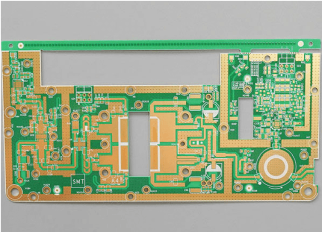
KKCPB specializes in manufacturing High Frequency PCBs using Rogers, PTFE, and hybrid stackup technologies, delivering reliable RF PCB solutions for telecommunications, aerospace, automotive radar, and industrial wireless systems.
Core Engineering Challenges
| Engineering Challenge | Root Cause | Engineering Impact |
|---|---|---|
| High insertion loss above 10 GHz | Dielectric loss and copper roughness | Reduced RF efficiency and transmission distance |
| Impedance discontinuity | Hybrid material transitions | Increased reflection and degraded signal integrity |
| Phase mismatch | Dielectric thickness variation | Beamforming errors and channel imbalance |
| Delamination in hybrid stackups | Different CTE values between materials | Reliability failures during thermal cycling |
| EMI coupling | High-density RF layout | Crosstalk and degraded receiver sensitivity |
| Manufacturing complexity | Mixed material lamination | Lower production yield and higher cost |
These challenges become particularly significant in 5G RF Front-End Modules, Microwave Module PCBs, Automotive Radar PCBs, and Satellite Communication PCBs, where electrical tolerances are measured in micrometers and fractions of a decibel.
Material Science & Dielectric Performance
Selecting the appropriate laminate depends on operating frequency, insertion loss targets, thermal requirements, and budget. Hybrid stackups allow designers to place premium RF materials only where necessary while using conventional laminates for digital and power circuits.
Comparison of High Frequency PCB Materials
| Material | Typical Dk | Typical Df (@10 GHz) | Primary Applications | Engineering Advantages |
|---|---|---|---|---|
| Rogers RO4350B | 3.48 | 0.0037 | 5G RF Modules, Power Amplifiers | Excellent balance of cost and RF performance |
| Rogers RO3003 | 3.00 | 0.0013 | Phase-critical RF Circuits | Outstanding phase stability |
| PTFE PCB | 2.1–2.6 | <0.0010 | Microwave & mmWave Systems | Ultra-low insertion loss |
| Hybrid Rogers + FR-4 | Customized | Optimized | Mixed RF/Digital Systems | Reduced overall manufacturing cost |
| Hybrid PTFE + High-Tg FR-4 | Customized | Optimized | RF Front-End Modules | Improved thermal and mechanical stability |
Compared with conventional FR-4, Rogers and PTFE materials provide significantly lower dielectric loss, tighter impedance control, and more stable electrical performance across wide temperature and frequency ranges.
KKCPB Case Study — Hybrid Stackup PCB for 5G RF Front-End Module
Client & Application Context
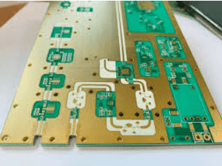
A global telecommunications equipment manufacturer required a 10-layer High Frequency PCB for a compact 5G RF front-end module operating across 3.5 GHz and 28 GHz frequency bands.
The module integrated:
- Multi-band power amplifiers (PA)
- Low-noise amplifiers (LNA)
- RF filters and duplexers
- Beamforming control circuitry
- High-speed digital interfaces
- Antenna feed network
The customer sought a PCB solution that balanced RF performance with production cost while ensuring scalability for volume manufacturing.
Engineering Problem
The original all-PTFE design delivered excellent RF performance but introduced several manufacturing and cost challenges:
- High material cost increased overall BOM expenses
- Complex lamination reduced manufacturing yield
- Thermal expansion mismatch affected multilayer alignment
- Impedance variation exceeded ±5% after assembly
- Long lead times impacted production schedules
The customer required an optimized stackup without compromising RF performance.
KKCPB Engineering Solution
KKCPB proposed a hybrid Rogers/PTFE stackup engineered specifically for mixed RF and digital applications.
The solution included:
- PTFE laminates for critical 28 GHz RF transmission layers
- Rogers RO4350B for sub-6 GHz RF routing
- High-Tg FR-4 for digital control and power distribution
- Controlled impedance routing with ±2% tolerance
- Vacuum lamination for hybrid material bonding
- Low-profile copper foil to minimize conductor loss
- Optimized ground plane segmentation for EMI suppression
- Embedded impedance test coupons for production verification
Comprehensive design verification was completed using HFSS, ADS, TDR, and Thermal FEM simulations prior to fabrication.
Measured Results
| Parameter | Customer Requirement | KKCPB Result |
|---|---|---|
| Controlled Impedance | ±5% | ±1.6% |
| Insertion Loss @28 GHz | <0.35 dB/in | 0.24 dB/in |
| Return Loss (S11) | < –15 dB | –19.1 dB |
| Phase Deviation | <1° | 0.42° |
| EMI Coupling | Minimized | Reduced by 39% |
| Manufacturing Yield | >95% | 98.9% |
| Material Cost | Baseline | Reduced by approximately 18% |
Project Outcome
The hybrid stackup achieved RF performance comparable to an all-PTFE solution while significantly reducing manufacturing costs and improving production efficiency.
For the customer, the optimized PCB provided:
- Improved RF signal integrity
- Lower insertion loss across both frequency bands
- Stable phase consistency for beamforming
- Reduced PCB fabrication costs
- Faster production turnaround
- Higher manufacturing yield
- Greater supply chain flexibility
This project demonstrates how strategic material selection can optimize both engineering performance and procurement value.
Stackup Design & RF Implementation
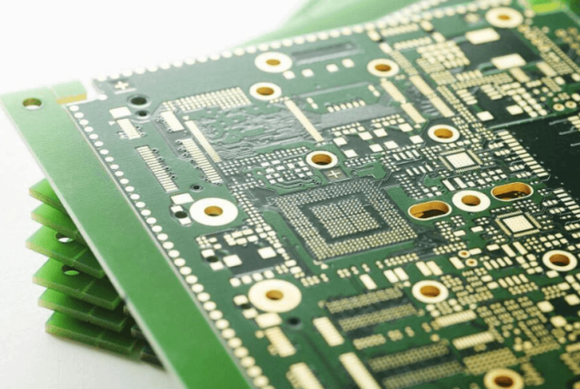
Representative 10-Layer Hybrid RF Stackup
| Layer | Function | Material |
|---|---|---|
| L1 | RF Signal | Rogers RO4350B |
| L2 | Ground Plane | Copper |
| L3 | RF Routing | PTFE Laminate |
| L4 | Ground Plane | Copper |
| L5 | High-Speed Digital | High-Tg FR-4 |
| L6 | Power Distribution | High-Tg FR-4 |
| L7 | RF Routing | Rogers RO4350B |
| L8 | Ground Plane | Copper |
| L9 | RF Signal | PTFE Laminate |
| L10 | Bottom Control Layer | High-Tg FR-4 |
Simulation & Validation
To ensure production-ready RF performance, KKCPB conducted comprehensive engineering verification throughout the design and manufacturing process.
HFSS Electromagnetic Simulation
- RF transmission path optimization
- Electromagnetic field distribution
- Coupling analysis
- Antenna feed network optimization
ADS Circuit Simulation
- S-parameter analysis
- Insertion loss prediction
- Phase matching validation
- RF network optimization
TDR Measurement
- Controlled impedance verification
- Via transition analysis
- Differential routing validation
Thermal FEM Analysis
- Heat distribution simulation
- Power amplifier thermal analysis
- Material expansion prediction
- Reliability evaluation during continuous operation
Inline AOI, X-ray inspection, impedance coupon testing, and vector network analyzer (VNA) measurements confirmed excellent agreement between simulation and manufactured PCB performance.
Environmental & Reliability Validation
| Test | Condition | KKCPB Result |
|---|---|---|
| Thermal Cycling | −40°C ↔ +125°C, 1000 cycles | No delamination or impedance drift |
| High Temperature Storage | 150°C, 1000 h | Stable dielectric performance |
| Humidity Test | 85°C / 85% RH, 1000 h | Dk variation <0.02 |
| Vibration Test | 5–500 Hz, 10G | No via cracking or solder fatigue |
| Lead-Free Solder Reflow | 260°C ×3 cycles | No warpage or layer separation |
| RF Performance Verification | Continuous operation at 28 GHz | Stable insertion loss and phase consistency |
These validation results demonstrate that hybrid Rogers/PTFE stackups can deliver long-term reliability in demanding RF environments while maintaining consistent electrical performance throughout the product lifecycle.
Engineering Summary & Contact
Selecting the right High Frequency PCB requires balancing electrical performance, manufacturability, and cost. While Rogers and PTFE materials each offer unique advantages, hybrid stackup technology enables engineers to achieve low-loss RF performance without the expense of an all-premium laminate design.
For procurement teams, hybrid stackups can reduce material costs, improve manufacturing yield, and shorten production lead times. For RF engineers, they provide the controlled impedance, phase stability, and EMI suppression necessary for modern 5G RF Front-End Modules, Microwave Communication Systems, Satellite Payloads, and Automotive Radar Platforms.
KKCPB specializes in High Frequency PCB manufacturing, offering comprehensive engineering support from material selection and stackup optimization to RF simulation, prototype fabrication, and high-volume production. Whether your project requires Rogers PCB, PTFE PCB, or a customized hybrid multilayer solution, our engineering team is ready to help you optimize performance, reliability, and total cost of ownership.
