multilayer PCB - KKPCB
 
HomeTag

multilayer PCB - KKPCB

Microvia PCB – High Density Interconnect PCB for Advanced Electronic Applications

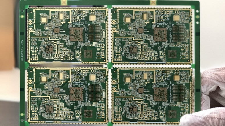
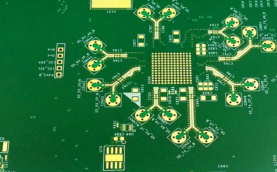
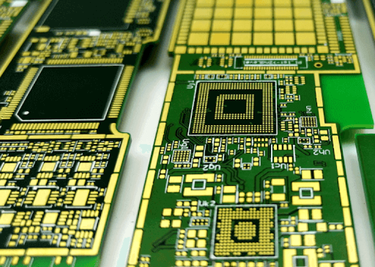
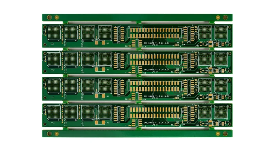
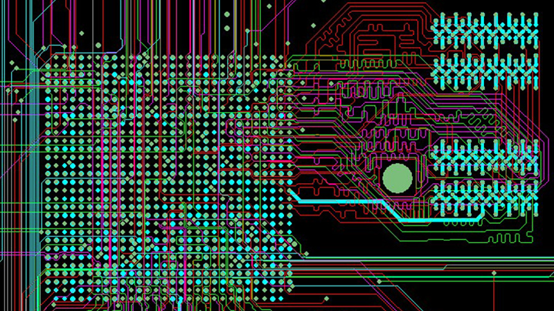
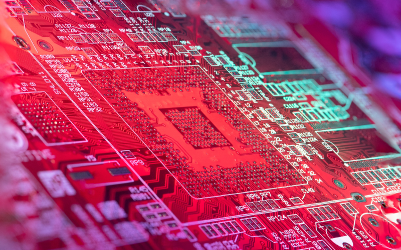
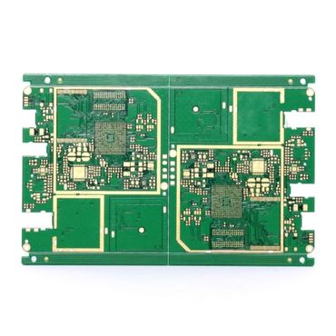
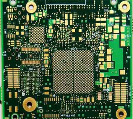
Microvia PCB for High Density Interconnect (HDI) Design As electronic products continue to shrink in size while increasing in functionality, traditional through-hole PCB structures are no longer sufficient. Microvia PCB technology enables higher routing density, improved signal integrity, and compact multilayer stackups, making it essential for modern high-performance electronics. Microvias are laser-drilled vias typically with...

Multilayer PCB – High Performance Multi Layer Printed Circuit Board for Advanced Electronics

What Is a Multilayer PCB? A Multilayer PCB is a printed circuit board composed of three or more conductive copper layers laminated together with insulating dielectric materials. Compared to single-sided or double-sided boards, Multilayer PCB technology allows significantly higher circuit density and more complex routing structures. Modern electronic systems increasingly require compact size, high speed...

Controlled Impedance PCB – High Speed PCB for Reliable Signal Transmission

What Is a Controlled Impedance PCB? A Controlled Impedance PCB is a printed circuit board engineered to maintain a precise and consistent impedance value along specific signal traces. Impedance control is critical in high speed and high frequency electronic systems where signal integrity directly affects performance and reliability. In modern electronic designs, signals travel at...

Buried Via PCB – Advanced Multilayer PCB with Internal Interconnection Technology

What Is a Buried Via PCB? A Buried Via PCB is a multilayer printed circuit board that contains vias connecting internal layers only, without reaching the outer surface layers. Unlike through-hole vias, buried vias are completely enclosed within the board stack-up. This allows designers to: Increase routing density Optimize outer layer space Improve signal integrity...

High Layer Count PCB – Advanced Multilayer PCB for High Density and High Speed Applications

What Is a High Layer Count PCB? A High Layer Count PCB refers to a multilayer printed circuit board typically built with 16 layers or more, and in advanced applications, up to 40, 60, or even higher layer counts. High Layer Count PCB is designed to support: High density routing Complex signal distribution Controlled impedance...

High TG PCB – High Glass Transition Temperature PCB for High Reliability Applications

What Is a High TG PCB? A High TG PCB is a printed circuit board fabricated using high glass transition temperature (TG) laminate materials, typically with TG values above 170°C, 180°C, or even 200°C depending on application requirements. The glass transition temperature (TG) refers to the temperature at which the PCB substrate transitions from a...

mmWave Module PCB – High Frequency PCB for 5G and Radar Applications

What Is an mmWave Module PCB? An mmWave Module PCB is a high frequency printed circuit board specifically designed for millimeter-wave applications (30–300 GHz), including: 5G communication modules Automotive radar systems High frequency IoT devices Satellite communication modules mmWave Module PCB ensures low signal loss, precise impedance control, and stable RF performance for high frequency...

High Speed Logic PCB Design and Manufacturing for High-Performance Digital Systems

What Is a High Speed Logic PCB? A High Speed Logic PCB is a printed circuit board designed to support high-speed digital logic circuits, where signal rise times are extremely fast and timing accuracy is critical. These PCBs ensure minimal signal distortion, precise timing, and reliable data transmission for high-performance computing, telecommunication, and semiconductor testing...

High Current PCB Manufacturing for Power Electronics and Industrial Applications

What Is a High Current PCB? A High Current PCB is a printed circuit board specifically designed to carry large currents while maintaining electrical stability and thermal reliability. These PCBs are commonly used in power electronics, automotive inverters, industrial automation, renewable energy systems, and high-current semiconductor testing. High current PCBs typically feature thick copper layers,...

Microvia PCB Manufacturing for High Density and High Performance Electronics

What Is a Microvia PCB? A Microvia PCB is a printed circuit board that uses microvias, which are very small drilled holes (typically <150 μm) to interconnect layers in high-density, multilayer HDI PCBs. Microvias enable fine-pitch routing, high pin count IC integration, and compact board layouts, making them essential for advanced electronics such as smartphones,...