multilayer PCB design - KKPCB
 
HomeTag

multilayer PCB design - KKPCB

Multilayer PCB: Advanced Design for High-Density and High-Speed Electronics

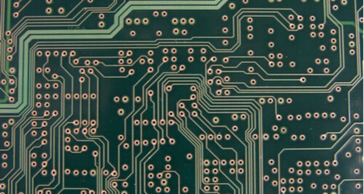
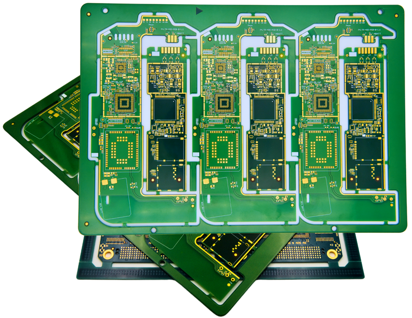
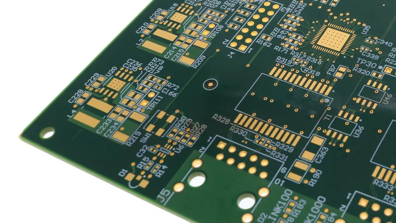
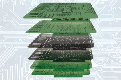
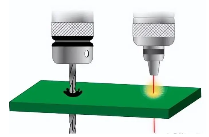
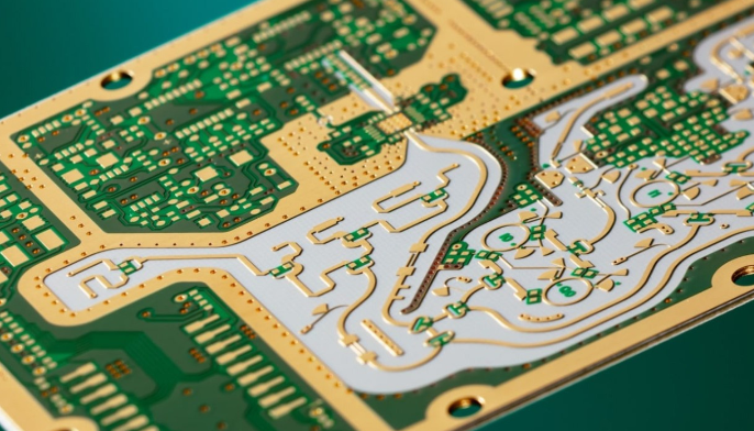
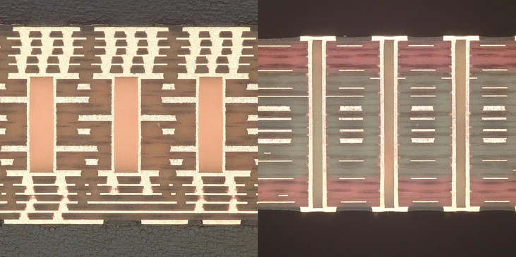
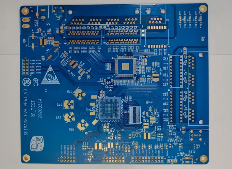
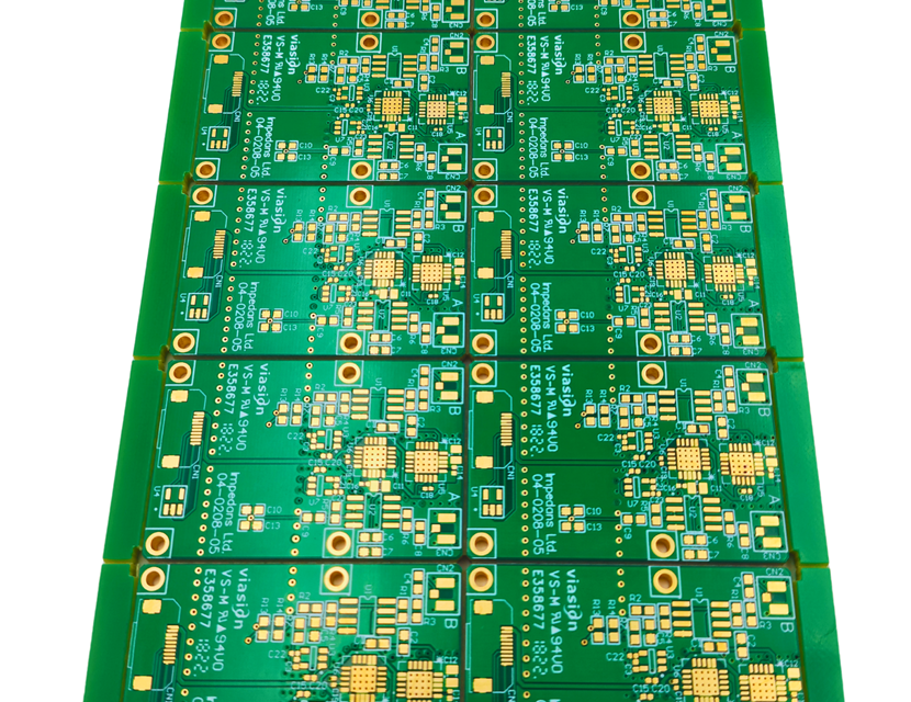
Multilayer PCB: Advanced Design for High-Density and High-Speed Electronics With modern electronic devices becoming increasingly compact and high-performance, Multilayer PCB technology is essential for achieving complex circuit routing, improved signal integrity, and efficient power distribution. A multilayer PCB consists of three or more conductive copper layers laminated together with dielectric materials , enabling compact, high-density,...

Fine Line PCB: High-Density Circuit Design for Advanced Electronics

Fine Line PCB: High-Density Circuit Design for Advanced Electronics As electronic devices continue to become smaller, faster, and more integrated, traditional PCB manufacturing technologies are often insufficient to meet the demands of modern circuit density. Fine Line PCB technology enables the creation of extremely narrow traces and spaces, allowing engineers to design highly compact and...

Why Multilayer PCBs Are Essential for High-Speed and High-Density Electronics

As electronic devices continue to evolve toward higher performance and smaller form factors, traditional two-layer circuit boards are no longer sufficient for many modern applications. This is where multilayer PCBs play a crucial role. By integrating multiple conductive layers into a single compact structure, multilayer PCBs enable engineers to design complex circuits while maintaining signal...

Multilayer Test PCB: Design, Manufacturing, and Applications

A Multilayer Test PCB is a specialized printed circuit board designed for testing, validation, and performance verification of electronic components, integrated circuits, and complex systems. Compared with standard PCBs, multilayer test boards incorporate multiple conductive layers to support high-density routing, signal integrity analysis, and accurate electrical testing. With the rapid development of modern electronics such...

Multilayer PCB: Structure, Benefits, and Applications in Modern Electronics

What Is a Multilayer PCB? A multilayer PCB is a printed circuit board composed of multiple copper layers separated by prepreg and core materials. Unlike single-sided or double-sided PCBs, multilayer boards provide additional routing layers, allowing engineers to design high-density circuits with improved electrical performance. Typical multilayer PCB configurations include: 4-layer PCB 6-layer PCB 8-layer...

Designing High Layer Count PCBs for Complex Signal, Power, and Thermal Integrity Challenges

As electronic systems continue to integrate higher data rates, greater power density, and tighter form factors, high layer count PCBs have become a foundational platform for modern hardware architecture. Designs exceeding 16, 20, or even 30 layers are now common in data center equipment, telecommunications infrastructure, aerospace electronics, and industrial control systems. However, increasing layer...

Enhance Signal Integrity and Thermal Reliability in Multilayer Blind Via PCBs for High-Density RF Modules

High-density RF modules in 5G base stations, satellite payloads, and advanced IoT systems require compact multilayer PCBs with precise signal routing, minimal crosstalk, and high thermal resilience. Blind via technology allows for efficient vertical interconnects while reducing PCB stackup thickness, improving high-frequency performance, and maintaining signal integrity across densely packed layers. KKPCB integrates precision lamination,...

Maximize RF Channel Integrity and Minimize Signal Loss with Blind Via PCB Architectures for High-Speed Communication Modules

High-speed communication modules in 5G, satellite transceivers, and high-frequency computing systems demand extreme precision in signal routing and interconnect integrity. As layer density increases and modules become more compact, traditional through-hole vias introduce unwanted parasitic effects, signal reflection, and EMI interference, compromising both channel fidelity and system performance. Blind via PCB technology enables selective inter-layer...

PCB Prototyping Services

In modern electronics development, PCB prototyping services play a critical role in transforming circuit concepts into functional hardware. Whether for high-speed PCB design, RF PCB development, or industrial electronics, fast and accurate PCB prototype manufacturing ensures design validation, reduces risks, and accelerates time-to-market. Professional PCB prototyping services provide engineers with rapid turnaround, high-quality fabrication, and...