Multi-layer PCBs - KKPCB
 
HomeTag

Multi-layer PCBs - KKPCB

PCB Layout Best Practices: Essential Design Considerations for Reliable Electronic Products

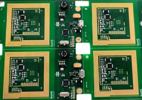
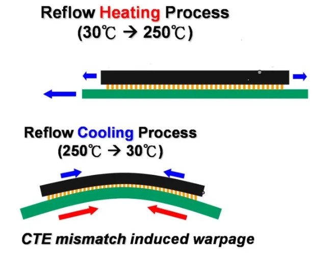
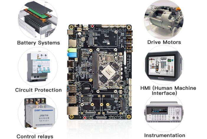
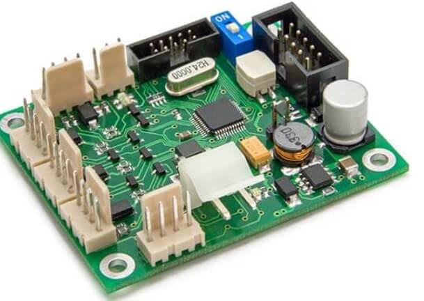
PCB design translates electrical schematics into a functional product, and its quality directly impacts production efficiency and product reliability. For beginners, mastering PCB layout can be challenging despite familiarity with design software, and common issues often arise. Here, seasoned engineers from KKPCB share their PCB layout insights to help avoid these pitfalls and inspire best practices. Component Placement...

PCB Materials: Building Blocks of Electronic Devices

Printed circuit boards (PCBs) are at the heart of modern electronic devices, powering everything from smartphones to aerospace systems. The journey of PCB materials has evolved significantly since their inception in the early 20th century. This article explores the composition, types, and advancements of PCB materials, essential for understanding the foundation of today’s electronic innovations. Evolution...

PCB Warpage: Causes, Prevention & Solutions Explained

When designing and manufacturing Printed Circuit Boards (PCBs), one common yet often overlooked issue is warpage. Warping occurs when the PCB bends or twists, leading to alignment issues during assembly. This deformation can cause misalignment of components, poor solder joints, and even failure of the final product. In this article, we will explore what causes PCB warpage,...