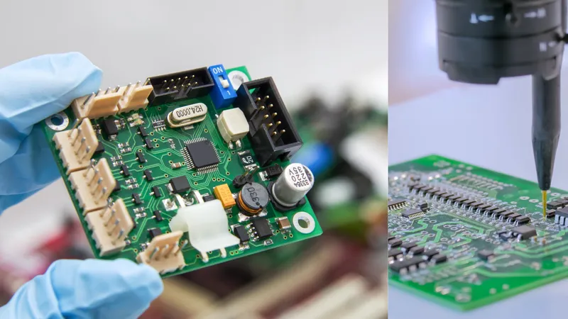
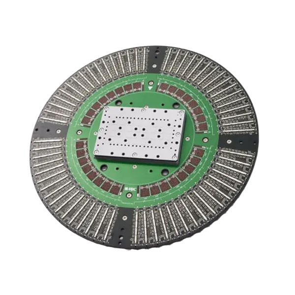
KKPCB - KKPCB
 
HomeTag

KKPCB - KKPCB

Multilayer Test PCBs: Ensuring Reliability in Complex Electronics

Multilayer PCBs are the backbone of modern electronics, from high-speed communication modules and industrial sensors to automotive and aerospace systems. Before committing to full-scale production, engineers rely on multilayer test PCBs to validate designs, assess signal integrity, and identify potential manufacturing challenges. These test boards simulate the full stack-up of the final product, allowing for...

HDI PCBs: Unlocking High-Density Performance for Modern Electronics

High-Density Interconnect (HDI) PCBs are a key technology for today’s compact and high-performance electronics. With fine lines, microvias, blind and buried vias, and multiple layers, HDI PCBs allow designers to fit complex circuits into small form factors, supporting applications from mobile devices to 5G infrastructure, automotive electronics, aerospace systems, and industrial IoT devices. Advanced Design...

Buried Via PCBs: Advanced Techniques for High-Density Multilayer Boards

Buried via technology has become essential in modern PCB design, particularly for high-density, high-performance applications. Unlike through-hole vias that pass through all layers, buried vias connect only internal layers, leaving outer layers uninterrupted. This allows designers to maximize routing space, improve signal integrity, and achieve compact, multilayer PCB layouts. Design Advantages Maximizing Board Real Estate:By...

High Layer Count PCBs: Design Challenges and Manufacturing Solutions

High Layer Count PCBs (printed circuit boards with 8 layers or more) have become a cornerstone in advanced electronics design. From telecommunications and medical devices to automotive and aerospace systems, these boards allow engineers to pack more functionality into smaller footprints while maintaining high performance. However, as layer counts increase, both design and manufacturing complexities...

RF Transceiver PCB: Key Design Technologies for Reliable Wireless Communication

In today’s connected world, RF transceiver PCB design plays a critical role in enabling stable and efficient wireless communication systems. From IoT devices to advanced communication infrastructure, high-performance RF PCB design ensures signal integrity, low interference, and reliable data transmission. Understanding the key design technologies behind RF transceiver PCBs is essential for achieving optimal performance....

Low Loss PCB for High-Frequency and High-Speed Signal Applications

As modern electronic systems operate at increasingly higher frequencies and faster data rates, signal loss has become a major challenge in PCB design. Low Loss PCBs are specifically engineered to minimize signal attenuation and maintain signal integrity in high-speed and high-frequency circuits. Unlike conventional FR-4 boards, low loss PCBs use advanced dielectric materials with lower...

Custom ATE PCB Design for Reliable Semiconductor Testing

Custom ATE PCB Automated Test Equipment (ATE) plays a critical role in modern electronics manufacturing, ensuring that integrated circuits, semiconductor devices, and electronic assemblies perform according to specification. At the heart of this process is the What Is a Custom ATE PCB? A Custom ATE PCB is a dedicated testing interface board designed to connect...

Multilayer Test PCB: Design, Manufacturing, and Applications

A Multilayer Test PCB is a specialized printed circuit board designed for testing, validation, and performance verification of electronic components, integrated circuits, and complex systems. Compared with standard PCBs, multilayer test boards incorporate multiple conductive layers to support high-density routing, signal integrity analysis, and accurate electrical testing. With the rapid development of modern electronics such...

Burn-in PCB Design and Manufacturing for High-Temperature Semiconductor Reliability Testing

A Burn-in PCB is a specialized test interface designed for accelerated semiconductor reliability screening under sustained electrical and thermal stress. In burn-in systems, the PCB is exposed to continuous high temperature, elevated voltage, and long operating cycles, making it one of the most mechanically and electrically stressed PCB types in semiconductor test environments. Unlike functional...

Taconic PCB Materials for Low-Loss, Stable Dielectric Performance in RF and High-Speed Systems

Taconic PCB materials are a class of engineered laminates specifically designed to address the challenges posed by high-frequency RF circuits, microwave systems, and high-speed digital signals. As system frequencies extend into multi-gigahertz and mmWave bands, dielectric loss, impedance variation, and phase instability become dominant constraints. Taconic PCB materials help engineers manage these constraints by delivering...