Internal Via PCB - KKPCB
 
HomeTag

Internal Via PCB - KKPCB

Buried Via PCB: Advanced PCB Design for High-Density and High-Speed Electronics

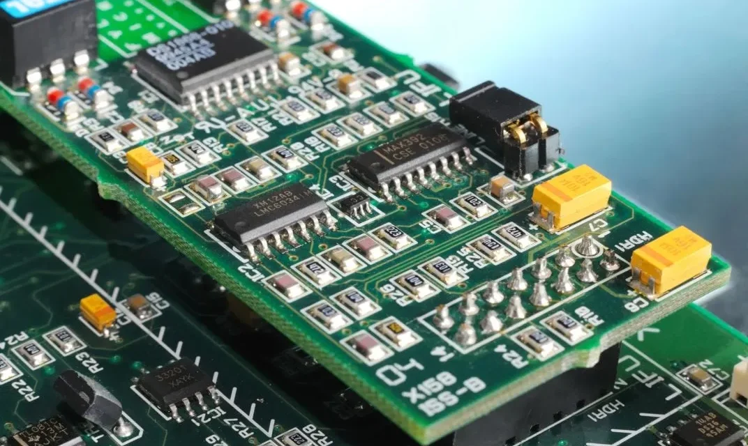
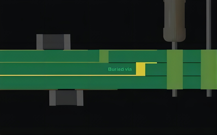
As electronic devices become smaller and more powerful, PCB designers face a constant challenge: fitting more circuitry into less space. Traditional through-hole vias can quickly consume valuable routing area, especially in multilayer boards. This is where Buried Via PCB technology becomes extremely useful. By placing vias entirely within internal layers, designers can maximize routing space...

Buried Via PCB – High Density Multilayer PCB with Internal Via Interconnection

What Is a Buried Via PCB? A Buried Via PCB is a multilayer printed circuit board that uses vias connecting only internal layers, without extending to the outer surface layers. Unlike through-hole vias that pass through the entire board thickness, buried vias are fully embedded within the PCB stack-up. This structure improves routing density, reduces...