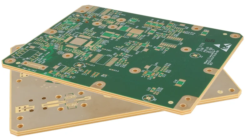
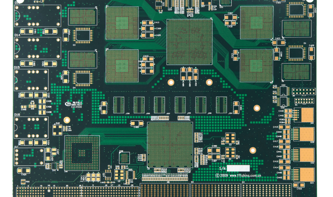
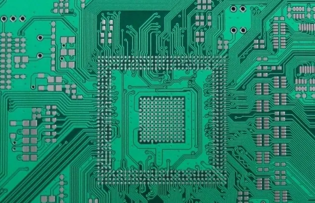
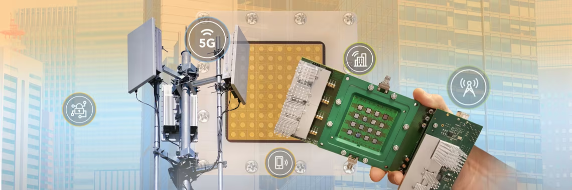
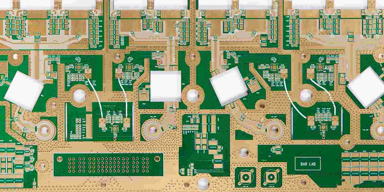
high-speed PCB - KKPCB
 
HomeTag

high-speed PCB - KKPCB

Multilayer PCB – Advanced Layered Circuit Board for High-Performance Electronic Systems

What Is a Multilayer PCB? A Multilayer PCB is a printed circuit board consisting of three or more conductive copper layers laminated together with insulating dielectric materials. These layers are electrically interconnected through plated vias to create complex routing structures within a compact footprint. Compared to single-layer or double-layer boards, multilayer PCBs enable higher circuit...

Microvia PCB – Laser-Drilled HDI Technology for High-Density Interconnection

What Is a Microvia PCB A Microvia PCB is a high-density interconnect (HDI) printed circuit board that uses laser-drilled microvias to connect adjacent copper layers. Unlike traditional mechanical through-holes, microvias are extremely small and typically connect only one or two layers. Microvia technology enables higher routing density, improved electrical performance, and more compact electronic designs....

Fine Line PCB – Precision Micro-Trace Technology for High-Density Circuit Design

What Is a Fine Line PCB? A Fine Line PCB refers to a printed circuit board manufactured with extremely narrow trace widths and spacing. Compared with standard PCB designs, fine line technology enables higher routing density within limited board space. Fine line PCBs are essential for modern electronic devices where compact size, high functionality, and...

High Density PCB Design – Engineering Solutions for Complex and Compact Electronic Systems

Engineering Challenges Behind High Density PCB As electronic systems become more compact and functionally integrated, PCB designers are facing increasing layout complexity. A High Density PCB is not simply about placing more components on a board — it requires precise coordination between electrical design, stack-up engineering, manufacturability, and long-term reliability. High density PCB development focuses...

Multilayer Test PCB – High Layer Count PCB for Precision Electronic Testing

What Is a Multilayer Test PCB? A Multilayer Test PCB is a high-layer-count printed circuit board specifically engineered for electronic testing and validation environments. It serves as a critical interface between testing equipment and the Device Under Test (DUT), ensuring accurate signal transmission and reliable measurement results. Unlike standard multilayer PCBs used in commercial products,...

HDI PCB – High Density Interconnect PCB for Advanced Electronic Applications

What Is an HDI PCB? An HDI PCB (High Density Interconnect PCB) is a printed circuit board designed with higher wiring density per unit area compared to traditional PCBs. It typically incorporates microvias, blind and buried vias, fine trace widths, and advanced multilayer stack-ups to support compact and high-performance electronic designs. HDI technology enables smaller...

Buried Via PCB – High Density Multilayer PCB with Internal Via Interconnection

What Is a Buried Via PCB? A Buried Via PCB is a multilayer printed circuit board that uses vias connecting only internal layers, without extending to the outer surface layers. Unlike through-hole vias that pass through the entire board thickness, buried vias are fully embedded within the PCB stack-up. This structure improves routing density, reduces...

High Speed PCB – Precision Design for Signal Integrity and High Data Rate Applications

High Speed PCB for Modern Digital Systems As data rates continue to increase in communication, computing, and semiconductor applications, PCB design must evolve to maintain signal integrity and stable performance. A High Speed PCB is specifically engineered to support high-frequency digital signals, fast edge rates, and high bandwidth transmission. Unlike standard PCBs, high speed boards...

UAV PCB – High Reliability PCB for Unmanned Aerial Vehicle Systems

UAV PCB for Advanced Drone and Aerial Systems A UAV PCB (Unmanned Aerial Vehicle PCB) is a high-performance printed circuit board used in drone systems to support flight control, real-time communication, navigation, and power distribution. UAV platforms demand compact size, lightweight construction, stable signal integrity, and resistance to vibration and temperature variation. As drone technology...

Multilayer PCB – High Performance Multi Layer Printed Circuit Board for Advanced Electronics

What Is a Multilayer PCB? A Multilayer PCB is a printed circuit board composed of three or more conductive copper layers laminated together with insulating dielectric materials. Compared to single-sided or double-sided boards, Multilayer PCB technology allows significantly higher circuit density and more complex routing structures. Modern electronic systems increasingly require compact size, high speed...