high-speed PCB - KKPCB
 
HomeTag

high-speed PCB - KKPCB

Designing Buried Via PCBs for High-Density Routing and Signal Integrity Optimization

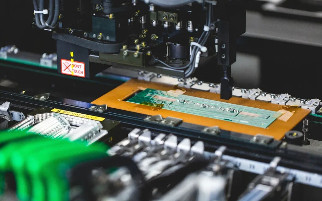
As electronic systems continue to evolve toward higher speed, smaller form factors, and increased functionality, traditional through-hole via structures are becoming a limiting factor. Buried Via PCB technology has emerged as a critical enabler for high-density routing and signal integrity optimization, particularly in HDI, high-speed digital, and RF applications. By embedding vias between inner layers...

From Stackup Planning to Lamination Control: Engineering High Layer Count PCBs That Actually Work

Engineering High Layer Count PCBs: Why “More Layers” Isn’t the Answer As electronic systems evolve toward higher speeds, higher integration, and smaller form factors, high layer count PCBs—typically 16 layers and above—have become standard in data centers, telecommunications, aerospace electronics, and advanced industrial systems. However, many multilayer PCBs fail not because of schematic errors, but...

Balancing Electrical Performance and Manufacturability in Buried Via PCB Structures

As electronic systems continue to evolve toward higher speeds, greater functionality, and reduced form factors, Buried Via PCB structures have become a critical enabler for advanced multilayer designs. By allowing interlayer connections without penetrating the outer layers, buried vias unlock higher routing density, improved signal integrity, and enhanced EMI control. However, these electrical advantages must...

Designing High Layer Count PCBs for Complex Signal, Power, and Thermal Integrity Challenges

As electronic systems continue to integrate higher data rates, greater power density, and tighter form factors, high layer count PCBs have become a foundational platform for modern hardware architecture. Designs exceeding 16, 20, or even 30 layers are now common in data center equipment, telecommunications infrastructure, aerospace electronics, and industrial control systems. However, increasing layer...

Controlled Impedance PCB Engineering for High-Speed Digital and High-Frequency RF Applications

A Controlled Impedance PCB is a critical foundation for modern high-speed digital systems and high-frequency RF applications. As signal rise times shrink and operating frequencies extend into multi-GHz ranges, PCB interconnects must behave as predictable transmission lines rather than simple copper connections. Controlled Impedance PCB design ensures signal integrity, phase stability, and EMI compliance across...

Enable Ultra-High Interconnect Density and Signal Integrity with Advanced High Layer Count PCB Architectures

High Layer Count PCB: The Backbone of Complex Electronic Systems A High Layer Count PCB refers to a multilayer printed circuit board typically featuring 16 layers, 24 layers, 32 layers, or more, designed to support complex signal routing, dense interconnections, and advanced power distribution. As electronic systems continue to integrate higher data rates, tighter form...

Enhance Routing Density and Signal Integrity with Buried Via PCB Architectures for High-Density Electronic Systems

Buried Via PCB: Enabling High-Density Interconnection Beyond Conventional Multilayer Boards A Buried Via PCB is a multilayer printed circuit board in which vias connect only internal layers and do not extend to the outer layers. Unlike through-hole vias, buried vias are completely embedded within the PCB stackup, enabling higher routing density, improved signal integrity, and...

Enable Ultra-Complex Routing and Signal Integrity with High Layer Count PCB Architectures for Advanced Electronic Systems

High Layer Count PCB: The Backbone of Ultra-Complex Electronic Integration A High Layer Count PCB refers to a multilayer printed circuit board typically exceeding 12 layers and extending to 20, 30, or even 60+ layers for advanced electronic systems. High layer count PCB designs are essential for applications requiring dense routing, high-speed signal transmission, controlled...

Optimize High-Frequency Signal Integrity and Power Efficiency with Low Dissipation Factor PCB Materials

Why Low Dissipation Factor PCB Matters in High-Frequency Electronics As electronic systems evolve toward higher frequencies, faster data rates, and tighter power budgets, signal loss within the PCB itself becomes a dominant performance constraint. In RF, microwave, mmWave, high-speed digital, and satellite communication systems, even minor dielectric losses can accumulate across long signal paths, directly...

Improve Thermal Reliability and Signal Integrity with High TG PCB Materials for High-Performance Electronic Systems

Engineering Context: Why High TG PCB Is Critical in Modern Electronics As electronic systems continue to push toward higher power density, faster signal speeds, and harsher operating environments, conventional PCB materials increasingly become a reliability bottleneck. Excessive heat, repeated thermal cycling, and dense component placement place enormous stress on standard laminates, often leading to warpage,...