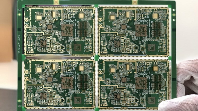
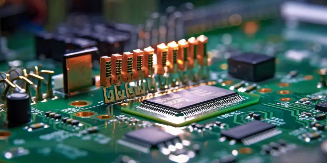
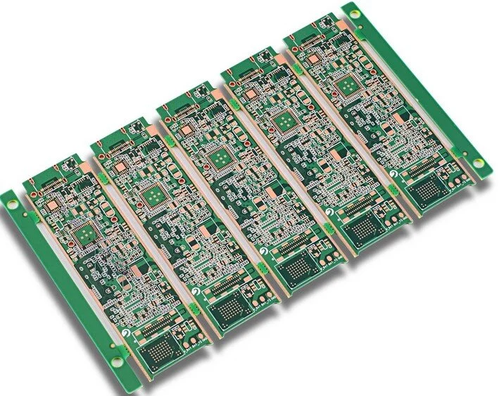
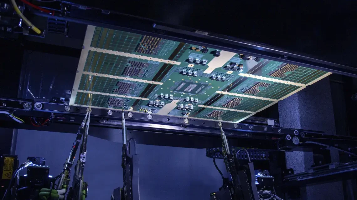
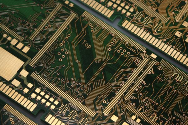
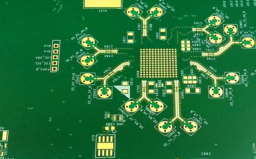
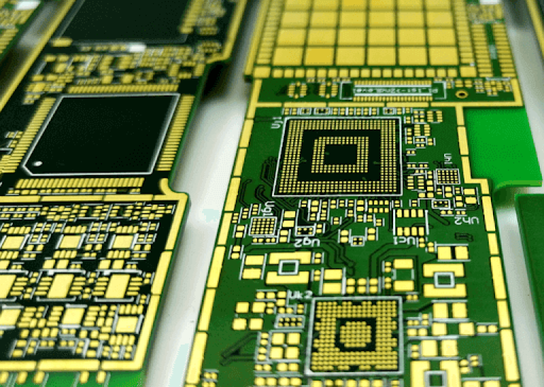
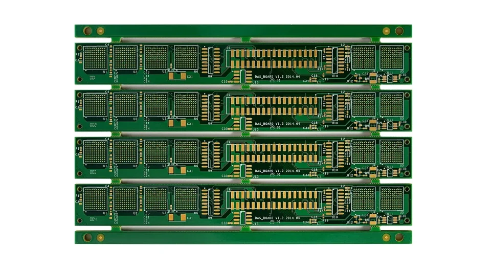
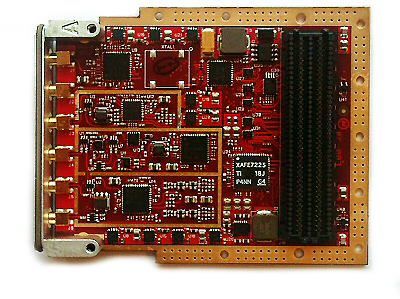
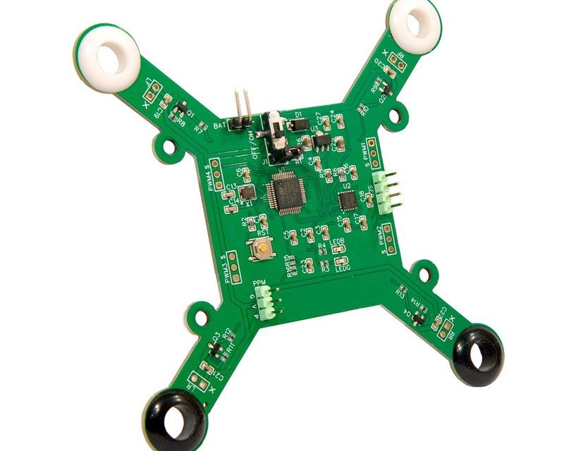
high-speed PCB - KKPCB
 
HomeTag

high-speed PCB - KKPCB

High Speed Logic PCB Design and Manufacturing for High-Performance Digital Systems

What Is a High Speed Logic PCB? A High Speed Logic PCB is a printed circuit board designed to support high-speed digital logic circuits, where signal rise times are extremely fast and timing accuracy is critical. These PCBs ensure minimal signal distortion, precise timing, and reliable data transmission for high-performance computing, telecommunication, and semiconductor testing...

Signal Integrity PCB Design and Manufacturing for High-Speed Applications

What Is a Signal Integrity PCB? A Signal Integrity (SI) PCB is a printed circuit board designed to maintain clean, stable high-speed signal transmission across digital, analog, or mixed-signal circuits. SI PCBs are essential for applications where data integrity, minimal signal distortion, and timing accuracy are critical, such as 5G communications, high-speed computing, automotive electronics,...

Microvia PCB Manufacturing for High Density and High Performance Electronics

What Is a Microvia PCB? A Microvia PCB is a printed circuit board that uses microvias, which are very small drilled holes (typically <150 μm) to interconnect layers in high-density, multilayer HDI PCBs. Microvias enable fine-pitch routing, high pin count IC integration, and compact board layouts, making them essential for advanced electronics such as smartphones,...

Multilayer PCB: Structure, Benefits, and Applications in Modern Electronics

What Is a Multilayer PCB? A multilayer PCB is a printed circuit board composed of multiple copper layers separated by prepreg and core materials. Unlike single-sided or double-sided PCBs, multilayer boards provide additional routing layers, allowing engineers to design high-density circuits with improved electrical performance. Typical multilayer PCB configurations include: 4-layer PCB 6-layer PCB 8-layer...

Low Loss PCB Manufacturing for High Frequency and High Speed Applications

What Is a Low Loss PCB? A Low Loss PCB is a printed circuit board designed with low dielectric loss materials to minimize signal attenuation during high-frequency and high-speed signal transmission. These PCBs are critical for applications where signal integrity, phase stability, and low insertion loss are essential. Low loss PCBs are widely used in...

Fine Pitch PCB Manufacturing for High Density and High Performance Applications

What Is a Fine Pitch PCB? A Fine Pitch PCB is a printed circuit board designed to support fine-pitch components, such as fine-pitch BGA, QFN, CSP, and high pin count ICs, where the spacing between pads and traces is extremely small. Fine pitch PCB technology is essential for modern electronics that demand high density, compact...

High Density PCB Manufacturing for Advanced Electronic Applications

What Is a High Density PCB? A High Density PCB (High Density Printed Circuit Board) is designed to accommodate more components, higher pin counts, and finer routing within a limited board area. It is widely used in applications that require compact size, high performance, and complex signal routing, such as semiconductor testing, telecommunications, automotive electronics,...

HDI PCB: High Density Interconnect PCB Manufacturing for Advanced Electronic Applications

An HDI PCB (High Density Interconnect PCB) is a key technology enabling compact, lightweight, and high-performance electronic products. As electronic devices continue to evolve toward smaller form factors, higher functionality, and faster data transmission, traditional PCB designs can no longer meet density and routing requirements. HDI PCB technology provides higher wiring density per unit area...

High Frequency IoT PCB Prototype: Key Materials, Design Challenges, and Manufacturing Solutions

High Frequency IoT PCB Prototype: Key Materials, Design Challenges, and Manufacturing Solutions With the rapid development of smart cities, industrial automation, and connected devices, IoT technology continues to evolve toward higher transmission speeds and wider communication bandwidths. High frequency IoT PCB prototypes play a crucial role in enabling stable wireless communication for applications such as...

Controlled Impedance PCB for High-Speed and High-Frequency Signal Integrity

What Is a Controlled Impedance PCB? A Controlled Impedance PCB is a printed circuit board designed to maintain a specified electrical impedance value along signal traces. Controlled impedance is critical for maintaining signal quality in high-speed, high-frequency, and RF electronic systems. In modern electronic devices, high data rate signals require precise impedance matching to prevent...