HDI PCB - KKPCB
 
HomeTag

HDI PCB - KKPCB

Probe Card Assembly PCB for Semiconductor Wafer Testing and ATE Applications

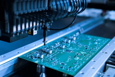
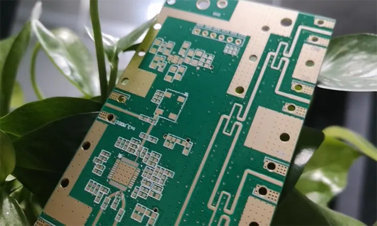
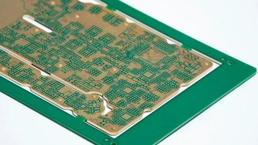
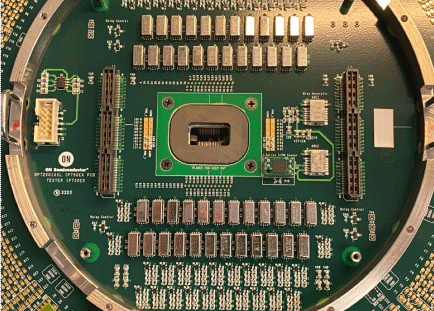
A Probe Card Assembly PCB is a highly specialized printed circuit board used in semiconductor wafer testing, acting as the critical electrical interface between the automated test equipment (ATE) and the device under test (DUT). It enables precise signal transmission from the tester to microscopic probe needles or MEMS probes that contact IC pads on...

High Pin Count PCB: Advanced PCB Solutions for High-Density and High-Reliability Applications

A High Pin Count PCB is designed to support electronic components with a large number of I/O pins, such as high-density BGAs, processors, FPGAs, and ASICs. As modern electronic systems demand higher performance, faster data transfer, and increased functionality, high pin count devices have become increasingly common. Manufacturing a reliable high pin count PCB requires...

HDI PCB: High Density Interconnect PCB Manufacturing for Advanced Electronic Applications

An HDI PCB (High Density Interconnect PCB) is a key technology enabling compact, lightweight, and high-performance electronic products. As electronic devices continue to evolve toward smaller form factors, higher functionality, and faster data transmission, traditional PCB designs can no longer meet density and routing requirements. HDI PCB technology provides higher wiring density per unit area...

Buried Via PCB for High-Density and Advanced Multilayer Circuit Designs

What Is a Buried Via PCB? A Buried Via PCB is a multilayer printed circuit board that uses vias connecting only internal layers without reaching the outer surface layers. These hidden interconnections allow designers to increase routing density while maintaining surface space for components and signal traces. Buried Via PCBs are widely used in HDI...

Blind Via PCB: High-Density Multilayer PCBs for Advanced Electronics

What Is a Blind Via PCB? A Blind Via PCB is a multilayer PCB that contains vias connecting an outer layer to one or more inner layers without going through the entire board. Unlike through-hole vias, blind vias enable high-density routing and space-saving designs, which are critical for HDI PCBs, high-frequency applications, and compact electronics....

OEM PCB Manufacturing: Customized and Reliable PCB Solutions

OEM PCB manufacturing is a critical part of modern electronics production, enabling companies to outsource PCB fabrication and PCB assembly (PCBA) while maintaining full control over product design and intellectual property. With increasing demand for custom PCB solutions, high reliability, and scalable production, OEM PCB services have become the preferred choice for companies seeking cost-effective...

High TG Materials for Thermal Reliability and Structural Stability in Advanced PCB Manufacturing

High TG materials play a decisive role in modern PCB designs where elevated operating temperatures, complex multilayer stackups, and long-term reliability are mandatory. As electronic systems continue to push higher power density and tighter integration, conventional low-TG laminates increasingly become a limiting factor in both manufacturing yield and field performance. Understanding the Importance of TG...

Taconic PCB Materials for High-Frequency, Low-Loss, and High-Speed RF Applications

Taconic PCBs are high-performance printed circuit boards engineered with low-loss dielectric laminates designed for RF, microwave, and high-speed digital applications. Taconic materials are widely recognized for their stable dielectric constant (Dk), low dissipation factor (Df), and thermal reliability, making them ideal for applications where signal integrity and frequency performance are critical. Key Advantages of Taconic...

Hybrid PCB Materials: Engineering Multi-Material Boards for Signal Integrity, Thermal Management, and Reliability

Hybrid PCB materials combine two or more substrate types—such as high-speed laminates, low-loss materials, BT epoxy, and ceramics—to create boards optimized for electrical performance, thermal management, and mechanical stability. Unlike single-material PCBs, hybrid designs allow engineers to tailor material properties to different areas of the circuit, achieving performance levels unattainable with conventional laminates. Why Hybrid...

High TG Materials Engineering for Thermal Stability and Reliability in Advanced PCB Designs

High TG materials are specialized PCB laminates and prepregs engineered to operate reliably under elevated temperatures, repeated thermal cycling, and high-density multilayer stackups. TG, or glass transition temperature, defines the point at which the resin matrix softens, directly affecting mechanical stability, dimensional integrity, and electrical performance. In advanced electronic systems, selecting high TG materials is...