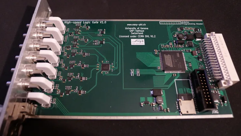
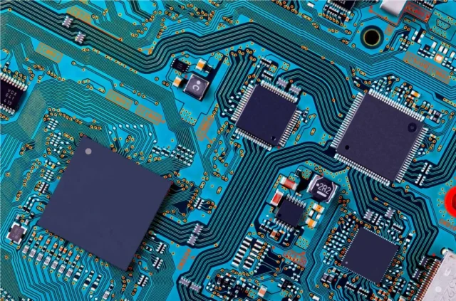
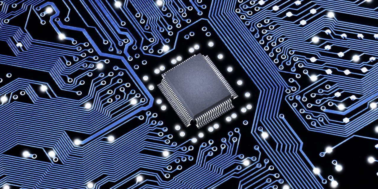
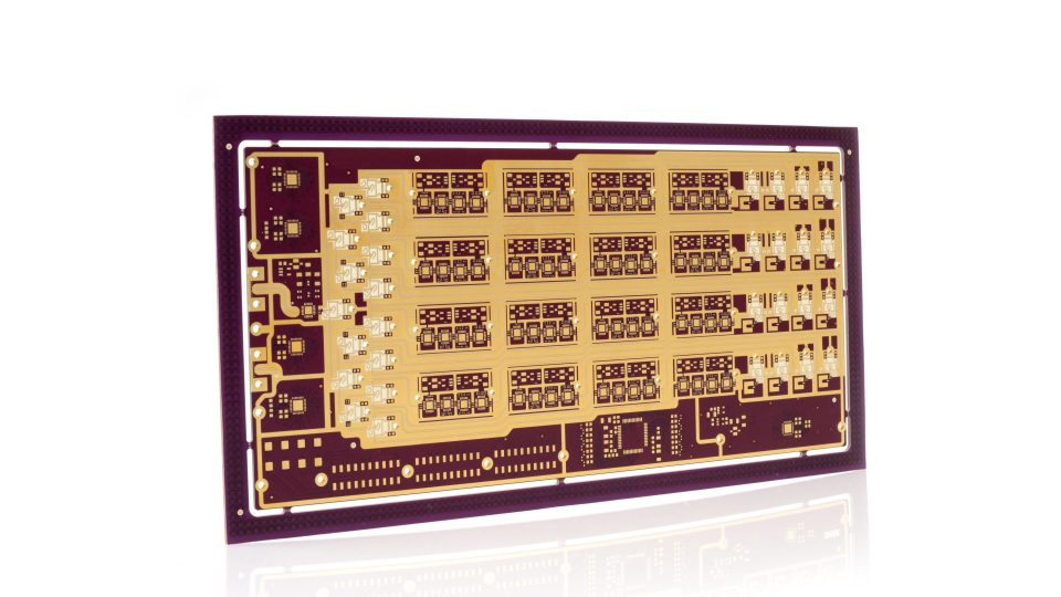
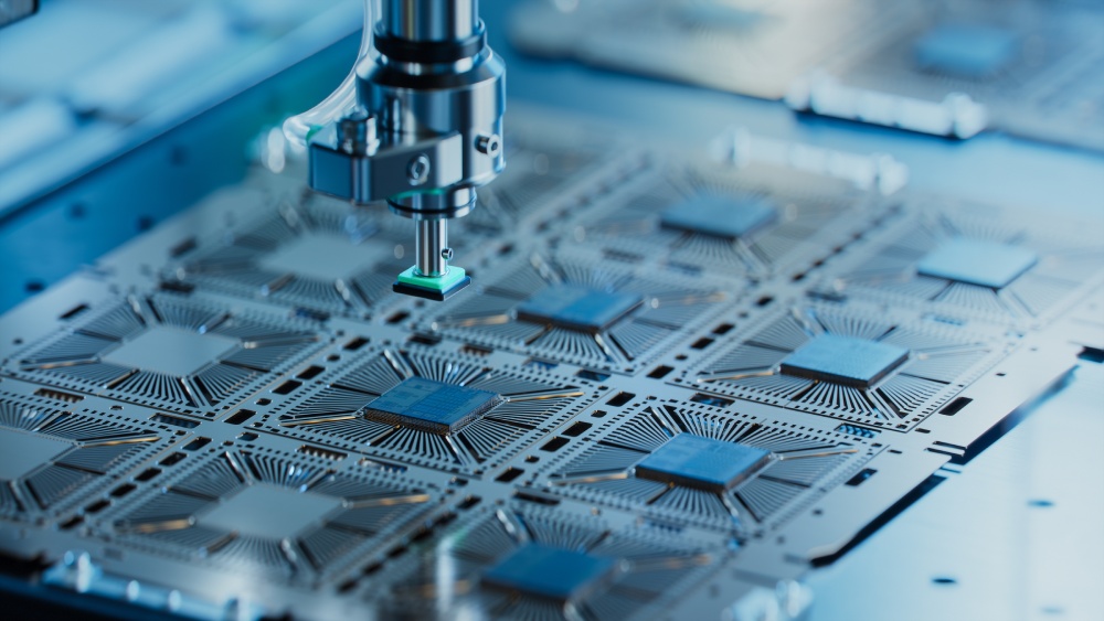
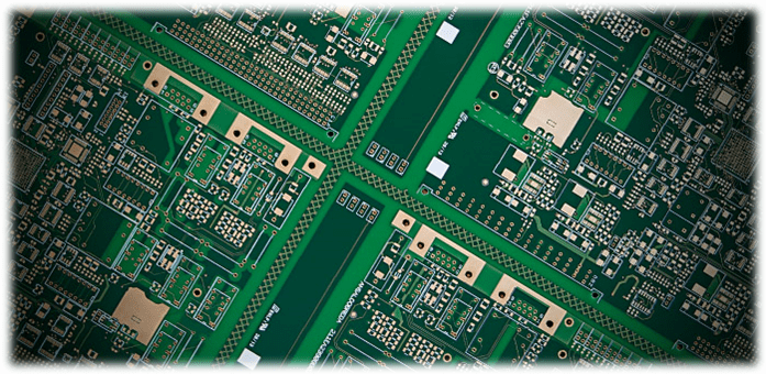
fine-pitch PCB - KKPCB
 
HomeTag

fine-pitch PCB - KKPCB

Multilayer PCB: Advanced PCB Solutions for Complex and High-Performance Electronics

A Multilayer PCB is a printed circuit board that contains three or more conductive layers, allowing designers to manage complex circuitry in a compact space. As electronic systems become more sophisticated, multilayer PCBs have become essential for applications requiring high-speed signal routing, dense component placement, and reliable power distribution. Multilayer PCBs are widely used in...

Fine Pitch PCB: Precision PCB Solutions for High Pin Count and Advanced IC Packaging

A Fine Pitch PCB is a high-precision printed circuit board designed to support fine pitch IC packages, such as fine-pitch BGA, QFN, CSP, and advanced semiconductor test sockets. As modern electronic devices continue to demand higher integration, smaller form factors, and faster signal speeds, fine pitch PCB technology has become essential for achieving reliable electrical...

High Density PCB: Advanced PCB Solutions for Compact and High-Performance Electronics

A High Density PCB is a specialized printed circuit board designed to support compact layouts, high pin count components, and complex signal routing within limited space. As electronic devices continue to shrink while increasing in performance, high density PCB technology has become essential for applications requiring high-speed data transmission, high-frequency signals, and reliable power delivery....

Probe Card Assembly PCB: Precision PCBs for Wafer-Level Semiconductor Testing

A Probe Card Assembly PCB is a critical semiconductor test PCB used in wafer-level testing to provide the electrical and mechanical interface between Automated Test Equipment (ATE) and semiconductor wafers. It supports probe needles or MEMS probes, routing test signals with extreme precision to ensure accurate electrical characterization before wafer dicing and packaging. As semiconductor...

Fine Pitch PCB: Precision PCB Solutions for High-Density Component Integration

A Fine Pitch PCB is a specialized printed circuit board designed for high-density ICs and compact electronic systems. Fine pitch technology supports components with very small pad spacing, allowing engineers to place high pin count ICs in limited PCB areas without compromising electrical performance. Fine pitch PCB design is crucial for modern applications like 5G...

High Density PCB: Advanced PCB Solutions for Compact, High-Performance Electronics

A High Density PCB (HDPCB) is a multilayer, fine-pitch printed circuit board designed to support compact electronic devices, high-speed digital systems, and high-frequency applications. HDPCBs are widely used in telecommunications, 5G, IoT, automotive electronics, and high-performance computing, where space constraints, high pin counts, and advanced signal integrity requirements demand precise PCB engineering. High density PCB...

High Pin Count PCB: Enabling Dense Interconnects for Advanced Semiconductor and High-Speed Systems

As semiconductor devices and high-performance modules continue to scale in complexity, the number of required electrical connections has increased dramatically. The High Pin Count PCB is designed to manage hundreds or even thousands of pins while maintaining signal integrity, mechanical reliability, and manufacturability. A well-designed High Pin Count PCB is critical for advanced computing, communication,...

High Pin Count PCB: Enabling Dense Interconnect and Reliable Performance in Advanced Electronics

 As electronic devices continue to integrate more functionality into smaller form factors, the number of signal, power, and ground connections has increased dramatically. The high pin count PCB is specifically engineered to support dense interconnect requirements while maintaining stable electrical and mechanical performance. From semiconductor testing to high-speed communication systems, a professionally manufactured high pin...

Probe Card PCB: Engineering Precision for High-Accuracy Wafer-Level Semiconductor Testing

Probe Card PCB: Engineering Precision for Wafer-Level Testing Introduction At the wafer-level test stage, the probe card PCB serves as the indispensable interface between automated test equipment (ATE) and the semiconductor wafer. As device geometries continue shrinking and electrical performance requirements become more demanding, precision test interfaces have become essential. The probe card PCB establishes...