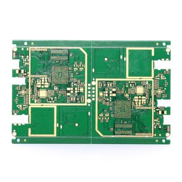
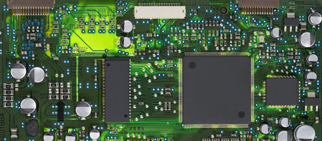
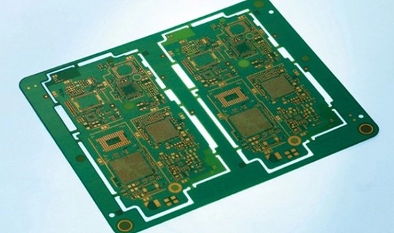
fine-pitch PCB - KKPCB
 
HomeTag

fine-pitch PCB - KKPCB

Fine Pitch PCB Manufacturing for High Density and High Performance Applications

What Is a Fine Pitch PCB? A Fine Pitch PCB is a printed circuit board designed to support fine-pitch components, such as fine-pitch BGA, QFN, CSP, and high pin count ICs, where the spacing between pads and traces is extremely small. Fine pitch PCB technology is essential for modern electronics that demand high density, compact...

High Density PCB Manufacturing for Advanced Electronic Applications

What Is a High Density PCB? A High Density PCB (High Density Printed Circuit Board) is designed to accommodate more components, higher pin counts, and finer routing within a limited board area. It is widely used in applications that require compact size, high performance, and complex signal routing, such as semiconductor testing, telecommunications, automotive electronics,...

BT Epoxy PCB Design for High-Reliability IC Packaging and High-Density Interconnect Applications

A BT Epoxy PCB is a material system specifically developed to meet the demands of semiconductor packaging, IC substrates, and high-density interconnect structures. Unlike general-purpose FR-4, BT epoxy resin is engineered for environments where thermal stability, dimensional control, and long-term reliability are non-negotiable design constraints. Material Characteristics of BT Epoxy PCB BT epoxy, derived from...

BT Epoxy PCB Design for Dimensional Stability and Electrical Reliability in IC Packaging Applications

A BT Epoxy PCB is a specialized organic substrate widely used in IC packaging, semiconductor interposers, and high-density electronic modules. BT (Bismaleimide Triazine) epoxy resin materials are engineered to provide enhanced thermal stability, low moisture absorption, and excellent dimensional control, making BT Epoxy PCBs a preferred choice for fine-pitch and high-I/O-count packaging environments. Unlike standard...

Fine Line PCB: High Precision PCB Manufacturing for HDI and High-Density Routing

What Is a Fine Line PCB? A Fine Line PCB is a high-precision printed circuit board manufactured with ultra-thin trace width and tight trace spacing, enabling high-density routing for advanced electronic products. Compared with standard PCB technology, Fine Line PCB fabrication focuses on achieving smaller line/space (L/S), higher wiring density, and improved signal performance in...

Fine Line PCB: High-Density, High-Precision PCB Solutions for Advanced Electronics

What Is a Fine Line PCB? A Fine Line PCB is a printed circuit board designed with ultra-narrow traces and spacing, typically below 100 µm. This allows for high-density component placement, complex routing, and miniaturized PCB designs. Fine line PCBs are essential in high-speed digital, RF, 5G, IoT, and aerospace electronics, where both signal integrity...

High Speed Logic PCB: Optimized Design for Fast Digital Circuits and Reliable Performance

Introduction to High Speed Logic PCB A High Speed Logic PCB is designed to support ultra-fast digital circuits while maintaining signal integrity, low noise, and reliable operation. These PCBs are critical for modern electronics, where data rates and clock frequencies are continually increasing, such as in computing, networking, 5G communications, automotive ECUs, and IoT devices....

Signal Integrity PCB: Ensuring High-Speed, Low-Noise Performance in Advanced Electronics

What Is a Signal Integrity PCB? A Signal Integrity PCB is engineered to maintain clean, reliable, and distortion-free signal transmission in high-speed and high-frequency electronic systems. Signal degradation, crosstalk, and reflections can compromise system performance, especially in high-speed digital, RF, 5G, IoT, and high-performance computing applications. Signal integrity PCB design ensures consistent impedance, controlled trace...

Microvia PCB: Advanced HDI PCB Technology for Miniaturized and High-Performance Electronics

Introduction to Microvia PCB A Microvia PCB is a key enabling technology in HDI (High Density Interconnect) PCB manufacturing, designed to meet the increasing demands for miniaturization, high-speed signal transmission, and high component density. By using laser-drilled microvias, Microvia PCBs significantly reduce interconnect length, improve routing flexibility, and enhance overall electrical performance. Microvia PCB technology...

Differential Pair PCB: High-Speed PCB Design for Signal Integrity and Noise Reduction

What Is a Differential Pair PCB? A Differential Pair PCB is a specialized printed circuit board designed with paired traces carrying equal and opposite signals. This design minimizes electromagnetic interference (EMI), reduces signal crosstalk, and maintains high-speed signal integrity. Differential pair PCBs are critical in applications where accurate high-speed data transmission is required, such as...