Electronics Industry NewsCustomer CaseEngineering TechnologiesPCB DesignPCB ManufacturingPCB Materials
Enhance Power Handling and Phase Stability Through Advanced Satellite PCB Materials in Ka- and Ku-Band Transceiver Modules
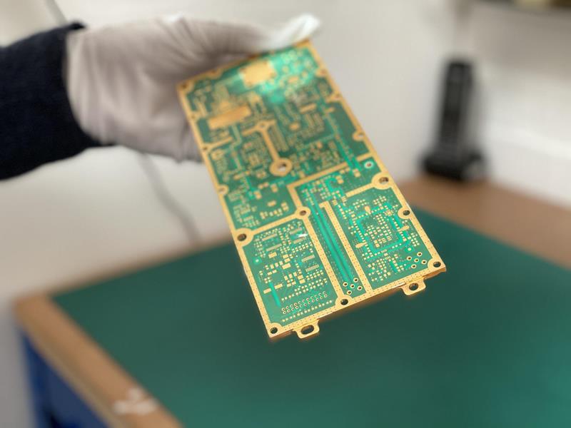
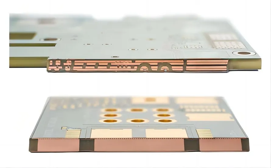
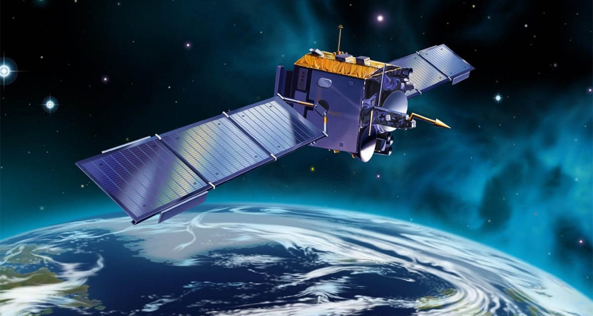
Ka- and Ku-band satellite transceivers demand high-frequency PCBs capable of handling elevated RF power while maintaining tight phase stability and low insertion loss. These modules operate in dense multilayer architectures, often within confined payloads, where thermal stress, EMI, and mechanical reliability directly impact signal fidelity and long-term performance. Advanced satellite PCB materials deliver low-loss dielectric...