
The Role of RF Transceiver PCB in Next-Generation Wireless Networks
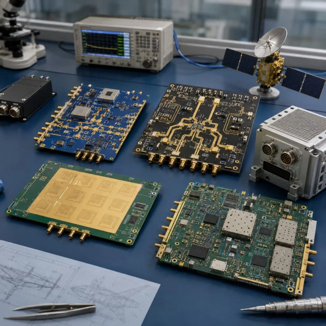
Modern 5G and emerging 6G communication systems require RF transceiver modules capable of supporting higher frequencies, wider bandwidths, and more complex multi-band operation. As wireless networks move toward mmWave frequency ranges, RF hardware must maintain excellent signal integrity, low insertion loss, phase stability, and thermal reliability under demanding operating conditions.
An RF Transceiver PCB serves as a critical platform for connecting RF components, antennas, power circuits, and control interfaces. Unlike conventional PCBs, RF transceiver boards must maintain predictable electrical performance at high frequencies, where even small variations in material properties, copper roughness, or impedance can significantly affect system performance.
Advanced RF transceiver PCB designs rely on:
- Low-loss dielectric materials
- Precise impedance control
- Optimized multilayer stack-up structures
- Effective thermal management
- EMI and crosstalk suppression
These factors are essential for maintaining reliable communication performance in 5G massive MIMO, mmWave modules, and future wireless systems.
Key Engineering Challenges in RF Transceiver PCB Design
1. Thermal-Induced Performance Variation
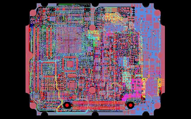
High-power RF transceiver modules generate significant heat during operation. Temperature variations can affect dielectric properties, mechanical expansion, and impedance consistency.
Common challenges include:
- Thermal-induced impedance drift
- CTE mismatch between materials
- Phase variation during temperature changes
Potential impacts:
- Phase misalignment
- Reduced gain efficiency
- Signal degradation
Effective solutions include optimized stack-up design, thermal via structures, and materials with stable thermal characteristics.
2. Minimizing Insertion Loss at mmWave Frequencies
At frequencies such as 28 GHz, 39 GHz, and beyond, signal loss becomes a critical factor affecting RF efficiency.
Major loss sources include:
- Dielectric dissipation
- Copper surface roughness
- Transmission line discontinuities
High-performance RF transceiver PCBs utilize:
- Low-Dk and low-Df laminates
- Smooth copper surfaces
- Optimized RF routing structures
These approaches help preserve signal strength and improve link performance.
3. Signal Integrity and Crosstalk Control
Dense RF layouts often contain multiple high-frequency signal paths within limited space, increasing the risk of interference.
Potential issues include:
- RF coupling between traces
- Crosstalk between channels
- Unstable return current paths
- EMI radiation
Design strategies include:
- Controlled trace spacing
- Optimized grounding structures
- Shielding via fences
- Dedicated RF reference planes
These techniques help maintain signal purity and improve system reliability.
4. Phase Stability for Multi-Band RF Applications
For advanced communication systems, phase consistency is critical for beamforming, antenna arrays, and massive MIMO applications.
Phase instability may result from:
- Material property variation
- Thermal expansion differences
- Manufacturing tolerances
Reliable RF transceiver PCB solutions require:
- Stable dielectric materials
- Precise layer alignment
- Tight impedance control
- Consistent manufacturing processes
Advanced RF PCB Material Considerations
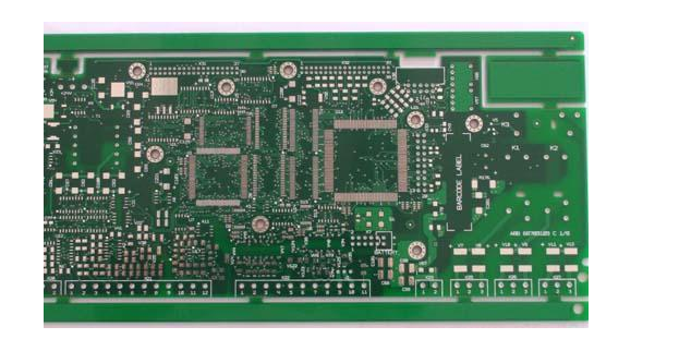
Material selection directly influences RF performance, especially in mmWave applications.
Key parameters include:
| Parameter | Typical Requirement | Engineering Benefit |
|---|---|---|
| Dk | Stable dielectric constant | Maintains impedance consistency |
| Df | Low dissipation factor | Reduces insertion loss |
| Thermal Conductivity | Enhanced heat dissipation | Supports high RF power operation |
| CTE | Controlled expansion | Improves phase stability |
| Moisture Absorption | Low moisture sensitivity | Maintains dielectric reliability |
Common material solutions include:
- High-frequency RF laminates
- PTFE-based materials
- Low-loss hybrid stack-ups
- High-Tg supporting layers
These materials enable stable RF performance under temperature and environmental variations.
KKPCB Engineering Case Study — 5G mmWave RF Transceiver PCB
Project Background
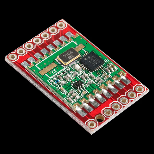
A telecom equipment manufacturer required a 6-layer RF transceiver PCB for 5G massive MIMO applications operating at 28–40 GHz.
Key requirements included:
- Low insertion loss
- Stable phase performance
- High RF power capability
- Reliable operation under thermal stress
KKPCB Engineering Approach
High-Frequency Stack-Up Optimization
- High-frequency laminate selection
- Controlled dielectric thickness
- Precision multilayer lamination process
RF Signal Integrity Improvement
- Low-roughness copper processing
- Optimized microstrip and stripline structures
- Controlled impedance routing
Thermal and EMI Management
- Thermal via optimization
- Embedded power structures
- Ground segmentation and shielding design
RF Performance Verification
- TDR impedance verification
- HFSS electromagnetic simulation
- Phase and transmission performance analysis
Manufacturing and Validation Results
| Parameter | Target | Result |
|---|---|---|
| Insertion Loss @28 GHz | <0.35 dB/in | 0.32 dB/in |
| Phase Deviation | <0.5° | 0.42° |
| Thermal Rise | <8°C/layer | 6.5°C |
| EMI Reduction | >30% | 34% |
| Impedance Variation | ±3% | ±1.6% |
Reliability Validation
| Test | Condition | Result |
|---|---|---|
| Thermal Cycling | -40°C to +125°C, 1000 cycles | No delamination, stable phase performance |
| Vibration & Shock | 5–500 Hz, 10G | No structural failure |
| Humidity Testing | 85°C / 85% RH, 1000 h | Stable dielectric performance |
| High-Power RF Operation | 28–40 GHz continuous operation | Minimal insertion loss variation |
| Solder Reflow | 260°C ×3 cycles | Stack-up integrity maintained |
Manufacturing Requirements for High-Performance RF Transceiver PCBs
Reliable RF transceiver PCB production requires:
- High-frequency laminate processing capability
- Precision multilayer fabrication
- Controlled impedance manufacturing
- Low-roughness copper technology
- RF simulation and verification support
- Thermal reliability control
These manufacturing capabilities ensure consistent RF performance from prototype development to volume production.
Conclusion: Enabling Reliable 5G and Future 6G RF Systems
The RF Transceiver PCB is a key foundation for modern wireless communication systems. As 5G and 6G technologies move toward higher frequencies and greater integration, PCB performance directly influences signal quality, thermal reliability, and system efficiency.
Through advanced RF materials, optimized stack-up design, impedance control, EMI mitigation, and precision manufacturing, high-performance RF transceiver PCBs enable stable operation for mmWave communication, massive MIMO, and next-generation wireless networks.
Selecting an experienced RF Transceiver PCB manufacturer helps communication equipment developers achieve reliable RF performance, faster validation cycles, and improved product competitiveness.
