EMI control - KKPCB
 
HomeTag

EMI control - KKPCB

Balancing Electrical Performance and Manufacturability in Buried Via PCB Structures

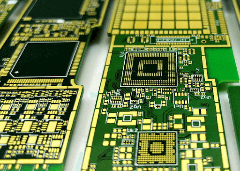
As electronic systems continue to evolve toward higher speeds, greater functionality, and reduced form factors, Buried Via PCB structures have become a critical enabler for advanced multilayer designs. By allowing interlayer connections without penetrating the outer layers, buried vias unlock higher routing density, improved signal integrity, and enhanced EMI control. However, these electrical advantages must...

Reduce Electromagnetic Drift and Improve Wideband Sensitivity Through High Frequency Sensor PCB Engineering for Medical Diagnostic Sensors

Medical diagnostic sensors have shifted toward high-frequency, microwave-based detection architectures to improve resolution, penetration depth, and signal precision. High Frequency Sensor PCB platforms now form the RF backbone of sensing modules used in MRI coils, millimeter-wave tissue scanners, microwave breast-imaging units, vital-sign monitoring radars, and non-contact biomedical sensors. These RF sensor PCB systems require extremely...

Stabilize Wideband Impedance and Reduce Signal Drift Using RO4835 PCB Laminates in Mission-Critical Satellite Links

Satellite communication hardware depends on highly stable RF PCB materials capable of maintaining low-loss transmission, tight impedance control, and long-term dielectric stability under extreme environmental shifts. RO4835 PCB laminates—known for oxidation-resistant resin systems, stable Dk over temperature, and low insertion loss up to Ka-band—are frequently selected for mission-critical RF payloads, transceiver modules, phased arrays, and...

Enhance Signal Integrity and Power Density with RO4350B PCB Designs in 5G Smartphone RF Front-Ends

RO4350B PCB materials are widely deployed in 5G smartphone RF front-end modules because they provide a balanced dielectric profile, low-loss characteristics, and stable RF transmission up to sub-6 GHz and selected mmWave bands. Modern antenna arrays, PA/LPF modules, LNA chains, and tunable impedance networks face stringent constraints in signal integrity, power density, EMI coupling, and...

SiC PCB for High-Power Modules and Automotive Powertrain Systems

SiC PCB for High-Power Modules and Automotive Powertrain Systems SiC (Silicon Carbide) devices are reshaping high-power electronics. Their wide-bandgap characteristics—high breakdown voltage, fast switching, and elevated junction temperatures—push PCB substrates into thermal, electrical, and mechanical stress profiles that exceed the range of traditional FR-4 and generic high-Tg laminates.A SiC PCB supporting traction inverters, onboard chargers,...

High-frequency Wi-Fi 6/7 antenna modules in modern laptops demand PCBs that maintain low insertion loss, precise phase alignment, and robust EMI suppression within compact layouts. TLY-5 PCB laminates, with a dielectric constant of 3.45 ± 0.03 and dissipation factor of 0.0012 @10 GHz, provide low-loss RF transmission and dimensional stability essential for multi-band performance. KKPCB...

Low-Loss Transmission and EMI Control of Ceramic PCBs in Satellite Communication and High-Frequency Payload Units

Engineering Context / Abstract   In modern satellite communication systems, RF payload units demand precise signal transmission, minimal insertion loss, and robust EMI suppression. High-frequency payloads, including Ku- and Ka-band transceivers, operate under extreme thermal, vacuum, and radiation conditions, where even minor dielectric fluctuations can cause phase errors and signal degradation.   Ceramic PCB substrates,...