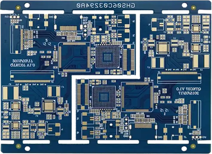
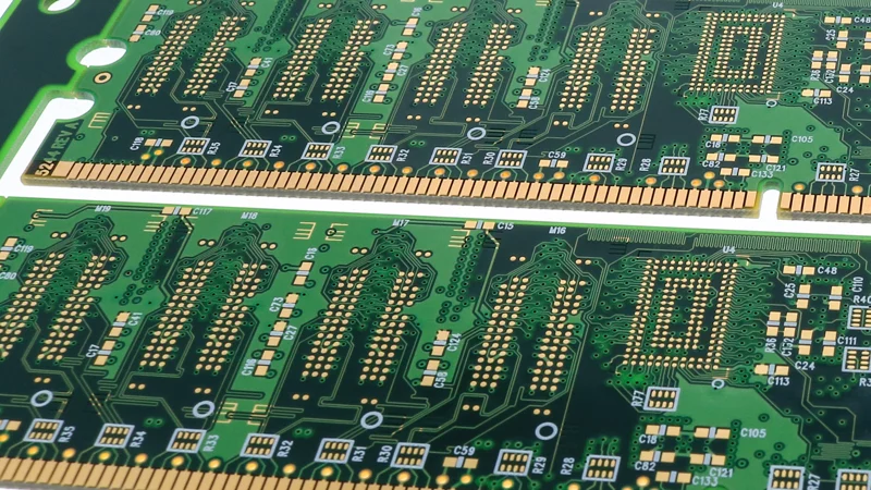
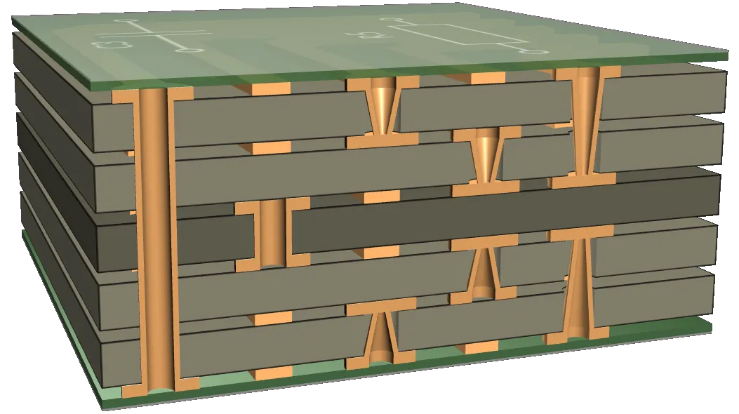
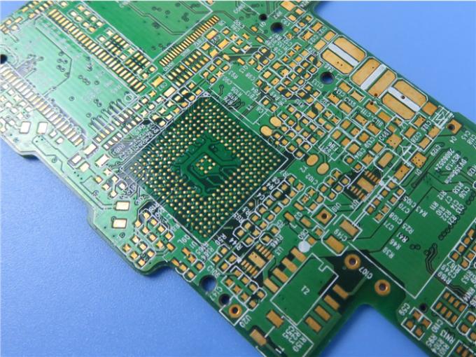
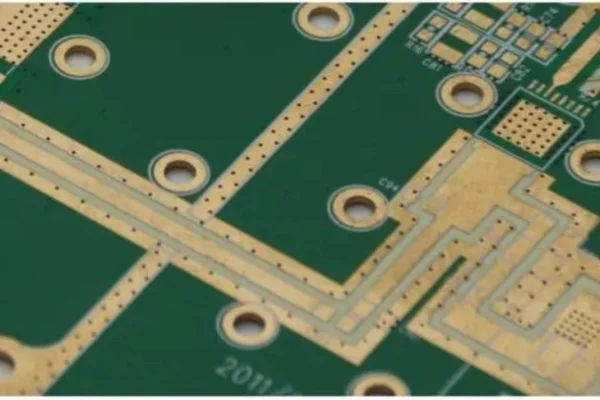
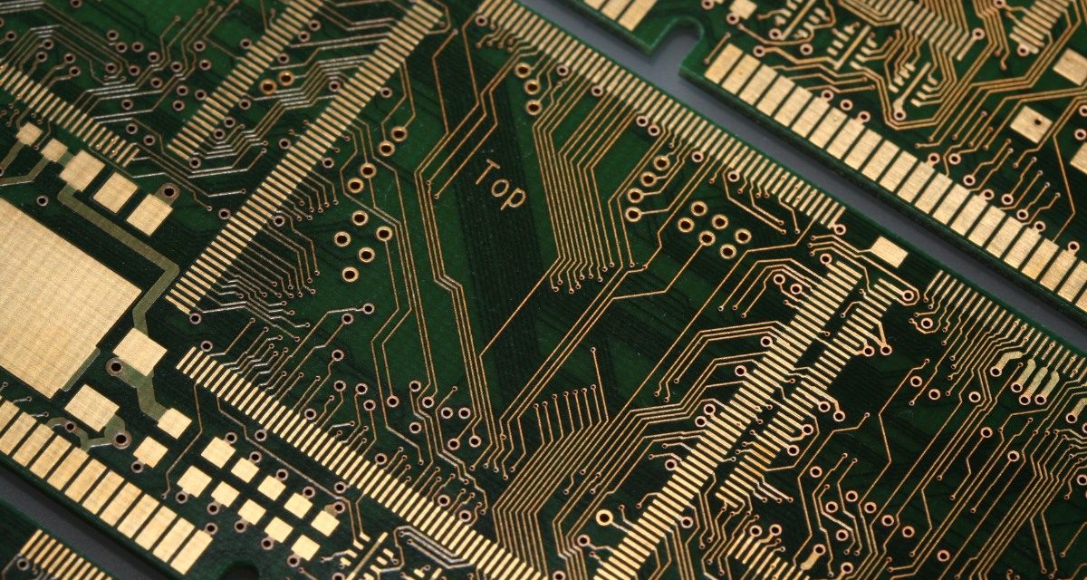
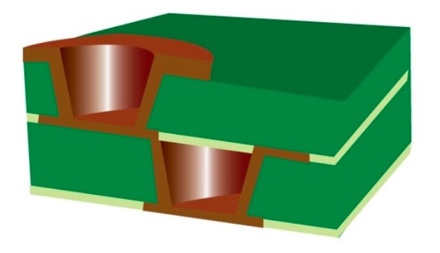
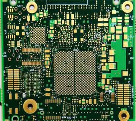
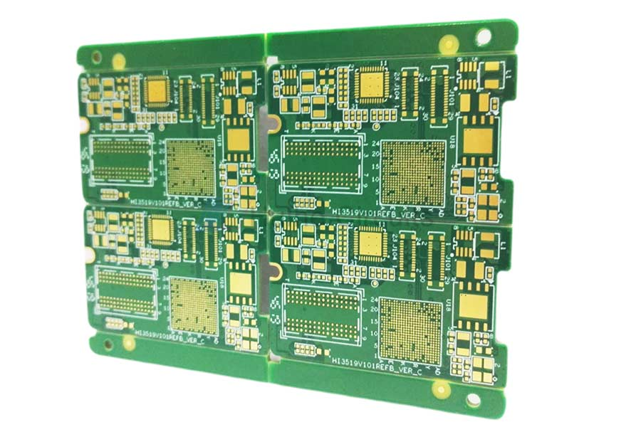
Blind Via PCB - KKPCB
 
HomeTag

Blind Via PCB - KKPCB

Microvia PCB: High-Density Interconnect Solutions for Advanced Electronics

Microvia PCB: High-Density Interconnect Solutions for Advanced Electronics As electronic devices become smaller, faster, and more complex, designers face increasing challenges in routing high-density circuits. Microvia PCB technology provides a solution by enabling high-density interconnects (HDI), allowing for compact multilayer designs with superior electrical performance. A Microvia PCB uses extremely small vias, typically less than...

HDI PCB: Design, Microvia Technology, and High-Density Applications

High Density Interconnect (HDI) PCB technology is designed to support modern electronic devices that demand higher performance, smaller form factors, and greater circuit complexity. HDI PCBs use advanced manufacturing techniques such as microvias, blind vias, buried vias, and fine line routing to increase the wiring density compared to traditional multilayer PCBs. As electronic products continue...

Blind Via PCB – High-Density Interconnect PCB for Advanced Electronics

What Is a Blind Via PCB? A Blind Via PCB is a type of multilayer printed circuit board where vias connect outer layers to one or more inner layers without passing completely through the board.Unlike through-hole vias, blind vias are partially embedded, allowing higher component density and more complex multilayer designs. They are widely used...

HDI PCB – High Density Interconnect PCB for Advanced Electronic Applications

What Is an HDI PCB? An HDI PCB (High Density Interconnect PCB) is a printed circuit board designed with higher wiring density per unit area compared to traditional PCBs. It typically incorporates microvias, blind and buried vias, fine trace widths, and advanced multilayer stack-ups to support compact and high-performance electronic designs. HDI technology enables smaller...

Microvia PCB – High Density Interconnect PCB for Advanced Electronic Applications

Microvia PCB for High Density Interconnect (HDI) Design As electronic products continue to shrink in size while increasing in functionality, traditional through-hole PCB structures are no longer sufficient. Microvia PCB technology enables higher routing density, improved signal integrity, and compact multilayer stackups, making it essential for modern high-performance electronics. Microvias are laser-drilled vias typically with...

HDI PCB – High Density Interconnect PCB for Advanced Electronics

What Is HDI PCB? HDI PCB (High Density Interconnect PCB) is a printed circuit board designed with higher wiring density per unit area compared to traditional multilayer PCBs. It uses advanced manufacturing technologies such as microvias, blind vias, buried vias, and fine line traces to achieve compact size and improved electrical performance. HDI PCB is...

Blind Via PCB – High Density Interconnect PCB for Compact and High Speed Designs

What Is a Blind Via PCB? A Blind Via PCB is a type of printed circuit board that contains vias connecting internal layers to one or more outer layers without passing completely through the board. Unlike through-hole vias, blind vias help: Reduce board size Increase routing density Optimize multilayer stack-ups Support HDI (High Density Interconnect)...

Blind Via PCB: High-Density Multilayer PCBs for Advanced Electronics

What Is a Blind Via PCB? A Blind Via PCB is a multilayer PCB that contains vias connecting an outer layer to one or more inner layers without going through the entire board. Unlike through-hole vias, blind vias enable high-density routing and space-saving designs, which are critical for HDI PCBs, high-frequency applications, and compact electronics....

High Density PCB: Advanced Solutions for Compact and High-Performance Electronics

A High Density PCB (HDPCB) is a printed circuit board designed to support compact, high-performance electronic systems. By leveraging HDI technology, microvias, blind/buried vias, and multilayer stackups, high density PCBs allow engineers to integrate more functionality into smaller footprints, making them essential for smart devices, high-speed computing, RF communication, and semiconductor testing. Key Features of...

Microvia PCB Technology for HDI, High-Speed, and Miniaturized Electronic Systems

What Is a Microvia PCB? A Microvia PCB is an advanced type of HDI (High Density Interconnect) printed circuit board that uses laser-drilled microvias, typically with a diameter of ≤150 μm, to interconnect PCB layers. Unlike traditional mechanical vias, microvias are designed for shorter signal paths, higher routing density, and compact layouts, making them essential...