advanced PCB design - KKPCB
 
HomeTag

advanced PCB design - KKPCB

Fine Line PCBs: Pushing the Limits of Precision and Density in Modern Electronics

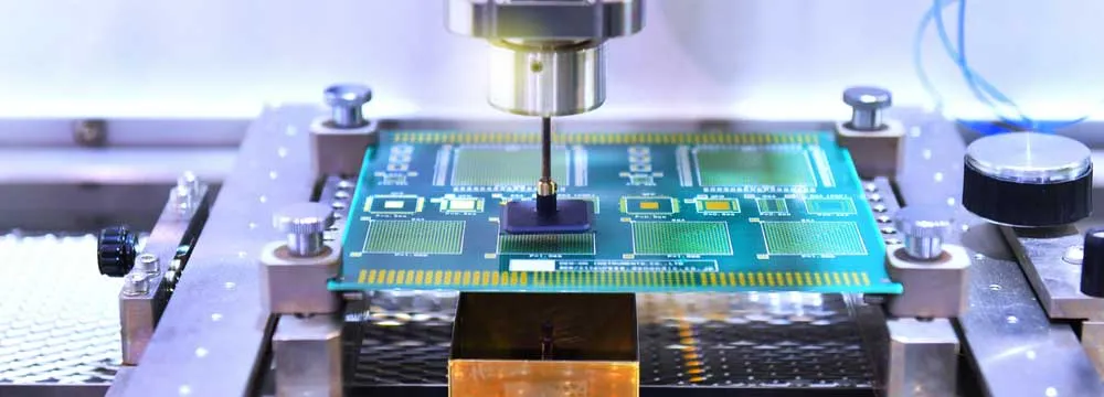
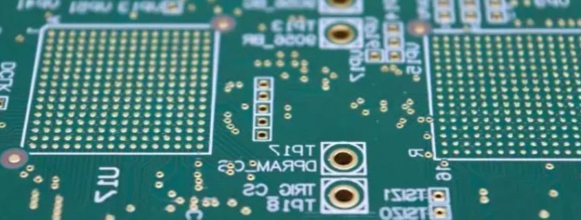
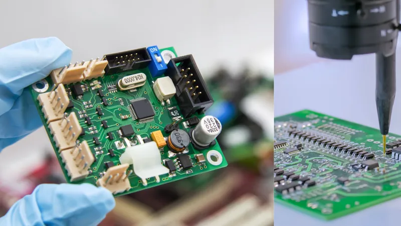
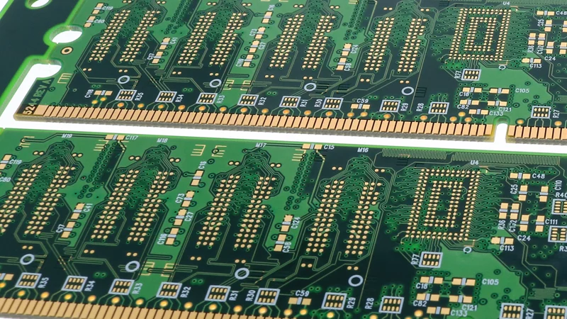
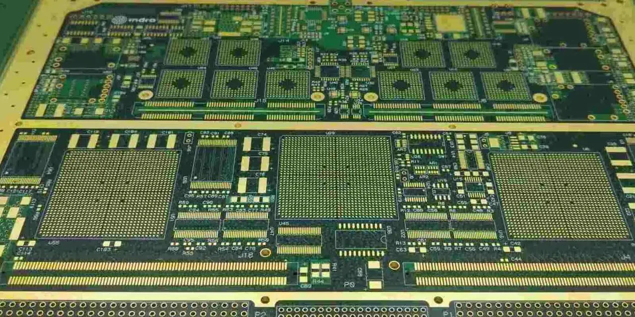
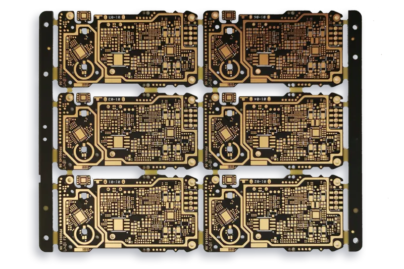
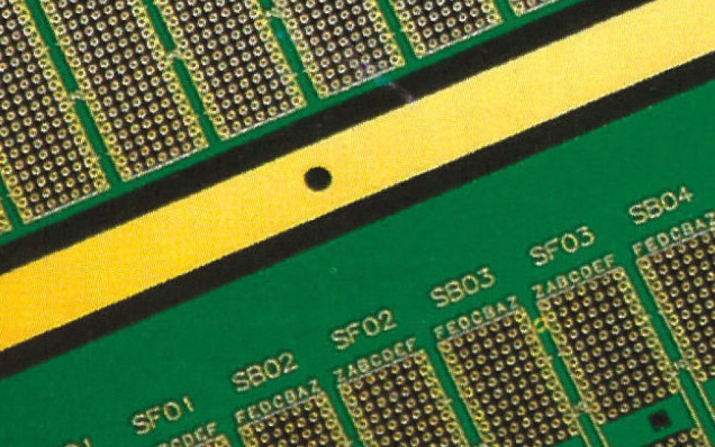
What Is a Fine Line PCB? A Fine Line PCB refers to a board manufactured with extremely narrow trace width and spacing, typically: ≤100 µm (4 mil) → standard fine line ≤75 µm (3 mil) → advanced ≤50 µm (2 mil) or below → ultra-fine line These geometries go beyond conventional PCB fabrication limits and...

High Pin Count PCBs: Managing Complexity in Advanced Electronic Systems

System Complexity as the Driving Force Modern electronic systems are no longer defined by individual components, but by highly integrated devices with massive I/O requirements. CPUs, GPUs, FPGAs, and advanced SoCs now feature hundreds to thousands of pins, driving the need for High Pin Count PCBs. This shift introduces a new level of complexity: Multiple...

HDI PCBs: High-Density Interconnect Solutions for Next-Generation Electronics

Why HDI PCBs Are No Longer Optional As electronic devices become smaller, faster, and more complex, traditional multilayer PCB designs struggle to keep up. HDI (High-Density Interconnect) PCBs address this challenge by enabling higher routing density, shorter signal paths, and better electrical performance. At the core of HDI technology is the use of: Microvias (laser-drilled...

High Pin Count PCBs: Enabling Complex Interconnections in Advanced Electronics

Why High Pin Count Matters As modern electronic systems evolve, integrated circuits such as CPUs, GPUs, FPGAs, and high-speed SoCs demand hundreds or even thousands of I/O connections. A High Pin Count PCB is designed to support these devices by enabling dense interconnections within limited board space. Unlike standard PCB designs, high pin count boards...

Buried Via PCBs: Strategic Layer Interconnects for High-Performance Designs

Why Buried Vias Matter As electronic systems become more compact and performance-driven, traditional via structures are no longer sufficient for complex routing requirements. A Buried Via PCB enables connections only between internal layers, eliminating unnecessary vertical paths through the entire board. This design approach is not just about saving space—it is about engineering control over...

High Layer Count PCBs: Advanced Solutions for Complex Electronic Systems

A High Layer Count PCB is a printed circuit board with 8 or more signal layers, often extending to 20–40 layers or more in advanced systems. These boards enable dense routing, compact design, and integration of multiple high-speed and RF circuits in a single assembly. High layer count PCBs are critical in: High-performance computing Networking...

Buried Via PCB: Advanced Multilayer Interconnects for High-Density Electronics

As electronic devices become smaller and more complex, the need for high-density interconnections within printed circuit boards increases. Buried via PCBs offer a solution by connecting inner layers without using surface space, allowing for compact, high-performance multilayer boards. Buried vias improve routing flexibility, signal integrity, and design density, making them critical for advanced applications such...

Multilayer HF PCB: High-Frequency Performance for Advanced Electronic Systems

As modern electronics push higher frequencies and data rates, high-frequency (HF) multilayer PCBs have become essential in enabling reliable and precise signal transmission. These PCBs are used in applications where low dielectric loss, controlled impedance, and minimal signal reflection are critical. Multilayer HF PCBs combine multiple layers of conductive and dielectric materials to achieve high-density...

Rigid-Flex PCB: Compact, High-Reliability PCB Solutions for Complex Designs

What Is a Rigid-Flex PCB? A Rigid-Flex PCB is a printed circuit board that combines rigid sections and flexible sections into a single unit. The rigid areas provide mechanical support and component mounting, while the flexible sections allow bending, folding, or flexing in compact assemblies. Rigid-Flex PCBs are widely used in high-reliability, space-constrained electronic devices,...

Designing Buried Via PCBs for High-Density Routing and Signal Integrity Optimization

As electronic systems continue to evolve toward higher speeds, smaller form factors, and increased functionality, traditional through-hole via structures are becoming a limiting factor. Buried Via PCB technology has emerged as a key solution for achieving high-density routing and optimizing signal integrity, especially in HDI, high-speed digital, and RF designs. By embedding vias between internal...