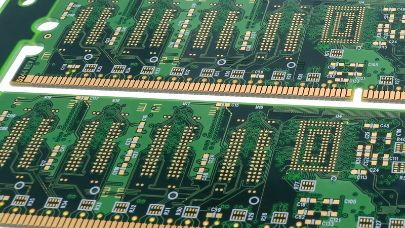
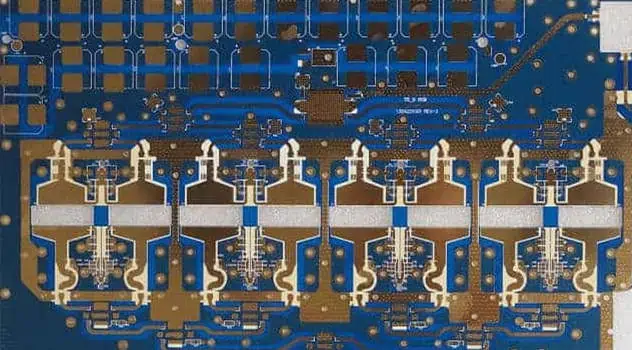
PCB Manufacturing Services | High-Quality PCB & PCBA - KKPCB
 
HomeCategory

PCB Manufacturing Services | High-Quality PCB & PCBA - KKPCB

Four Key Points in High-Speed PCB Design

When designing high-speed PCBs, process variations and other factors can significantly impact actual impedance. Automated design tools may not always detect these subtleties, making proactive, defensive design essential. Here’s how to address common challenges in high-speed PCB design. 1. Layer Stack-Up Configuration A well-configured layer stack-up is foundational for signal integrity (SI) and electromagnetic compatibility (EMC). Ideally,...

How to Design RF Circuits and PCB Layouts

This guide delves into the four fundamental characteristics of RF circuits—RF interface, small desired signals, large interference signals, and adjacent channel interference—and highlights essential considerations for PCB design. 1. RF Interface in RF Circuit Simulation Concept Overview: RF systems can be divided into two parts: baseband and RF. Baseband: Handles the input/output signal frequencies and enhances data transmission reliability. RF...

Characteristics of RF Interfaces and RF Circuits in PCB Design

RF (Radio Frequency) circuits and interfaces exhibit unique characteristics, requiring specialized design considerations. These challenges are due to the nature of RF signals and their interaction with physical elements of the circuit. Understanding these aspects ensures optimal performance in wireless communication systems. Below is an exploration of RF circuit characteristics, PCB design considerations, and optimization techniques. RF Interface...

Efficient Automatic PCB Wiring: Skills and Key Points

The rapid evolution of PCB design, with increasingly compact layouts, higher device densities, and stringent performance requirements, has necessitated the adoption of advanced EDA tools. However, achieving high routing efficiency and optimizing the design still requires strategic planning and manual intervention. This guide outlines practical skills and key points for efficient automatic PCB wiring, emphasizing design planning, layout,...

High-Frequency Circuit Design Solution Based on RT/duroid® 6010.2LM Material for Miniaturization

Discover the advantages of RT/duroid® 6010.2LM high-frequency PCB material for compact RF and microwave circuit designs. With a high dielectric constant (Dk 10.7), low loss tangent (0.0026 @10 GHz), excellent thermal stability, and superior mechanical properties, KKPCB helps you achieve miniaturized circuits with high signal integrity for 5G, satellite communications, and high-density PCBs.

High-Speed PCB Copy Board and Design Strategy

High-speed PCB design is crucial in fields like communication, computing, and graphics/image processing. Engineers in these areas often employ unique strategies tailored to their industry’s specific requirements. Below, we explore different approaches and key considerations for high-speed PCB design. 1. High-Speed PCB Design in Telecommunications In telecommunications, the design complexity is exceptionally high due to the...

The Critical Issue of Near Holes in Multi-Layer PCB Design

In multi-layer PCB design, the primary focus during routing is to ensure efficient and reliable electrical connections between layers using vias. However, as PCB density increases, vias often need to be placed closer together, leading to design and manufacturing challenges. These challenges not only complicate the production process but also impact the long-term reliability of the product....

Experience Sharing in Multi-Layer PCB Impedance Line Routing

With the rapid advancement of modern electronics, devices like smartphones, computers, and high-definition TVs rely heavily on the intricate design of circuit boards to achieve high-speed data transmission. A key component of this functionality is impedance matching, which ensures reliable and stable signal transmission. This article explores practical insights and best practices for impedance-controlled PCB routing,...

High-Speed PCB: Optimal Six-Layer Board Structure

When designing high-speed PCBs, the layer stack-up plays a crucial role in ensuring signal integrity, minimizing crosstalk, and achieving optimal electromagnetic compatibility (EMC). For a standard six-layer board with a thickness of 1.6mm, selecting the right structure can significantly impact performance. Below is an analysis of common six-layer board structures and their suitability for high-speed designs....

Basic Knowledge You Need to Master for PCB Design

PCB design is a critical part of developing electronic systems. It requires knowledge to ensure schematic correctness, signal integrity, minimal interference, and convenient connectivity. Below are key recommendations and optimized methods for PCB design. 1. Working with FPGA If the system involves an FPGA, you must verify the pin assignments using specialized software like Quartus II before creating...