PCB Design Services | Professional PCB Layout & Design - KKPCB
 
HomeCategory

PCB Design Services | Professional PCB Layout & Design - KKPCB

Custom Probe Card PCB: High-Precision Platforms for Stable and Repeatable Wafer Testing

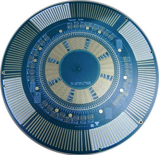
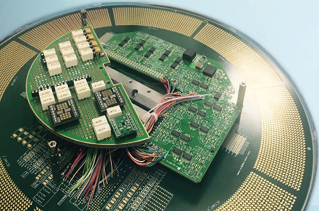
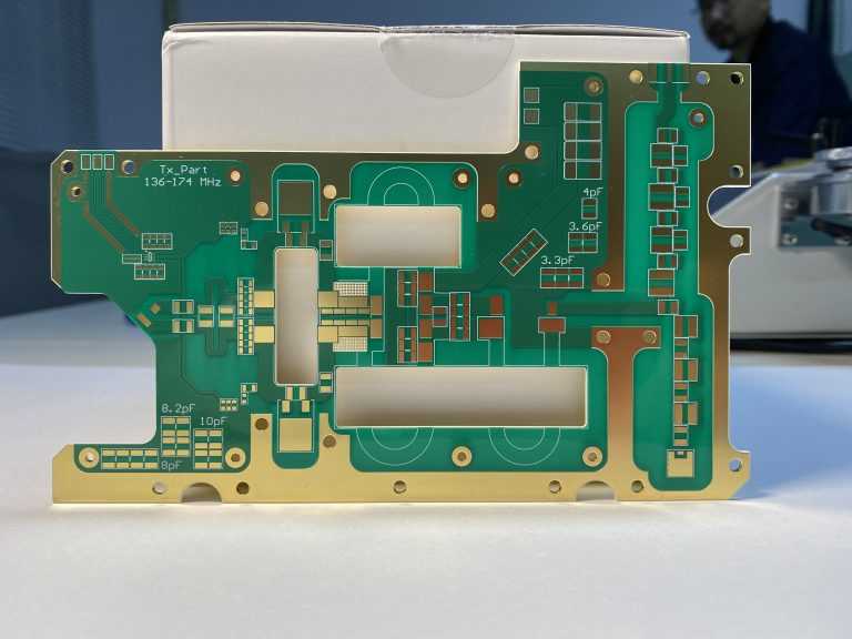
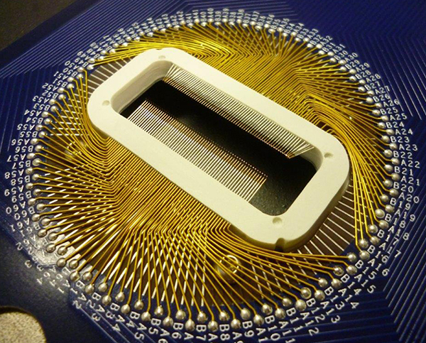
In wafer-level semiconductor testing, probe cards must deliver precise electrical contact across thousands of touchdowns while maintaining consistent signal performance. The Custom Probe Card PCB provides the structural and electrical foundation that supports probe arrays, ensuring accurate, repeatable wafer testing. A properly engineered custom probe card PCB directly impacts test yield, device characterization accuracy, and...

Custom ATE PCB: Engineering-Tested Boards for Stable and Repeatable Automated Testing

In automated semiconductor testing, accuracy must be maintained not just once—but across thousands of test cycles. A Custom ATE PCB is designed specifically to match the electrical, mechanical, and environmental requirements of each test platform, ensuring stable and repeatable test results over time. A professionally engineered custom ATE PCB reduces false failures, improves yield, and...

High Frequency Test PCB: Ensuring Measurement Accuracy in RF and Microwave Validation

In RF, microwave, and high-speed electronic testing, even minor PCB imperfections can introduce significant measurement errors. The High Frequency Test PCB is engineered to serve as a neutral and stable signal platform, allowing engineers to evaluate devices and systems with confidence. A properly designed high frequency test PCB ensures that test results reflect device performance—not...

Custom Probe Card PCB: Precision Interconnect Solutions for Wafer-Level Semiconductor Testing

Wafer-level semiconductor testing demands extreme accuracy, mechanical stability, and signal fidelity. The Custom Probe Card PCB serves as the core interconnect platform between automated test equipment and semiconductor wafers, enabling precise electrical contact and repeatable measurements. A professionally manufactured custom probe card PCB is essential for high-yield wafer testing. What Is a Custom Probe Card...

Custom ATE PCB: Tailored Test Board Solutions for High-Accuracy Automated Test Equipment

Automated Test Equipment (ATE) systems require test boards that deliver precise electrical performance and long-term reliability. A Custom ATE PCB is engineered specifically to match the electrical, mechanical, and functional requirements of each test platform, ensuring accurate and repeatable test results. A well-designed custom ATE PCB plays a critical role in advanced semiconductor and electronic...

High Frequency Test PCB: Precision Design and Low-Loss Materials for Accurate RF and High-Speed Testing

As RF, microwave, and high-speed digital technologies continue to advance, test environments must deliver exceptional signal fidelity. The High Frequency Test PCB is specifically designed to support precise signal transmission, minimal loss, and repeatable measurement results at high frequencies. A properly engineered high frequency test PCB is essential for reliable RF and high-speed validation. What...

Multilayer Test PCB: Reliable Signal Integrity and Power Control for Advanced Electronic Testing

Modern electronic testing systems demand accurate signal transmission, stable power delivery, and repeatable results. The Multilayer Test PCB is specifically designed to meet these requirements by integrating multiple signal, power, and ground layers into a compact and electrically optimized structure. A well-designed multilayer test PCB ensures consistent and reliable test performance. What Is a Multilayer...

HDI PCB: High-Density Interconnect Technology for Compact and High-Speed Electronic Designs

As electronic products continue to evolve toward smaller form factors and higher performance, conventional PCB technologies often reach their limits. The HDI PCB (High-Density Interconnect PCB) overcomes these limitations by enabling ultra-dense routing, shorter signal paths, and enhanced electrical performance. A professionally engineered HDI PCB is essential for modern high-speed and high-density electronic systems. What...

High Pin Count PCB: Advanced Routing and Reliability Solutions for Complex Electronic Systems

As integrated circuits continue to increase in complexity, the number of I/O connections per device has grown dramatically. The High Pin Count PCB is specifically engineered to accommodate dense signal routing, stable power delivery, and long-term reliability without compromising electrical performance. A professionally designed high pin count PCB enables advanced systems to function reliably under...

Test Socket PCB: High-Reliability Interface Boards for Repetitive Semiconductor Device Testing

In semiconductor testing, consistent electrical contact is essential for accurate and repeatable results. The Test Socket PCB serves as the mechanical and electrical foundation that supports test sockets, ensuring stable signal transmission between the device under test and the test system. A professionally engineered test socket PCB is critical for maintaining test accuracy throughout high-cycle...