PCB Design Services | Professional PCB Layout & Design - KKPCB
 
HomeCategory

PCB Design Services | Professional PCB Layout & Design - KKPCB

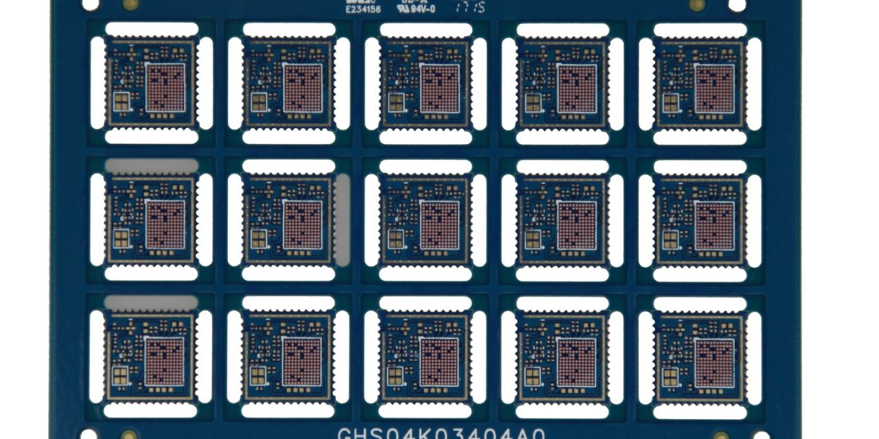
Multilayer Test PCB – High Layer Count PCB for Precision Electronic Testing

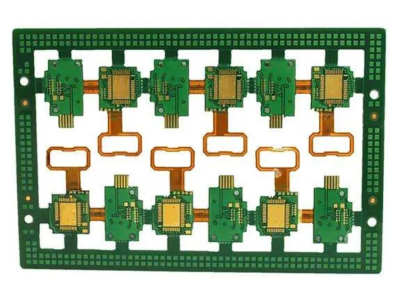
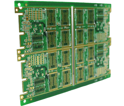
What Is a Multilayer Test PCB? A Multilayer Test PCB is a high-layer-count printed circuit board specifically engineered for electronic testing and validation environments. It serves as a critical interface between testing equipment and the Device Under Test (DUT), ensuring accurate signal transmission and reliable measurement results. Unlike standard multilayer PCBs used in commercial products,...

HDI PCB – High Density Interconnect PCB for Advanced Electronic Applications

What Is an HDI PCB? An HDI PCB (High Density Interconnect PCB) is a printed circuit board designed with higher wiring density per unit area compared to traditional PCBs. It typically incorporates microvias, blind and buried vias, fine trace widths, and advanced multilayer stack-ups to support compact and high-performance electronic designs. HDI technology enables smaller...

Load Board PCB – High Precision Interface Board for Semiconductor Testing

What Is a Load Board PCB? A Load Board PCB is a critical interface board used in Automated Test Equipment (ATE) systems for semiconductor device testing. It connects the tester to the device under test (DUT), transmitting signals, power, and measurement data with high accuracy and stability. Load boards are specifically engineered to support high...

ATE Test PCB – High Precision PCB for Automated Test Equipment Applications

ATE Test PCB for Semiconductor and IC Testing An ATE Test PCB (Automated Test Equipment PCB) is a high-precision printed circuit board designed for semiconductor and integrated circuit testing systems. It serves as the electrical interface between the test system and the device under test (DUT), ensuring accurate signal transmission, stable power delivery, and reliable...

Buried Via PCB – High Density Multilayer PCB with Internal Via Interconnection

What Is a Buried Via PCB? A Buried Via PCB is a multilayer printed circuit board that uses vias connecting only internal layers, without extending to the outer surface layers. Unlike through-hole vias that pass through the entire board thickness, buried vias are fully embedded within the PCB stack-up. This structure improves routing density, reduces...

Rigid-Flex PCB – Flexible and Rigid Hybrid PCB for Compact and High Reliability Applications

What Is a Rigid-Flex PCB? A Rigid-Flex PCB combines rigid circuit board sections with integrated flexible circuit layers into a single unified structure. This hybrid design allows the board to bend in specific areas while maintaining structural stability in others. Unlike traditional assemblies that connect separate rigid boards using cables or connectors, rigid-flex technology integrates...

Double Layer HF PCB – High Frequency Two Layer PCB for RF and Microwave Applications

Double Layer HF PCB for RF and Microwave Systems A Double Layer HF PCB (High Frequency PCB) is a two-layer printed circuit board designed specifically for RF and microwave signal transmission. Unlike standard double-sided FR4 boards, HF PCBs use low-loss, stable dielectric materials to ensure reliable signal performance at high frequencies. Double layer high frequency...

High TG PCB – High Glass Transition Temperature PCB for Thermal Stability and Reliability

What Is a High TG PCB? A High TG PCB refers to a printed circuit board manufactured using laminate materials with a high glass transition temperature (Tg). The glass transition temperature is the point at which the PCB substrate transitions from a rigid state to a softer, more flexible state under heat. Standard FR4 materials...

High Speed PCB – Precision Design for Signal Integrity and High Data Rate Applications

High Speed PCB for Modern Digital Systems As data rates continue to increase in communication, computing, and semiconductor applications, PCB design must evolve to maintain signal integrity and stable performance. A High Speed PCB is specifically engineered to support high-frequency digital signals, fast edge rates, and high bandwidth transmission. Unlike standard PCBs, high speed boards...

SiC PCB: Advanced PCB Solutions for High-Voltage and High-Temperature Power Applications

SiC PCB: Supporting the Next Generation of Power Electronics With the rapid growth of electric vehicles, renewable energy systems, and industrial power modules, Silicon Carbide (SiC) devices are becoming a key technology in modern power electronics. Compared to traditional silicon components, SiC devices operate at higher voltages, higher temperatures, and higher switching frequencies. However, these...