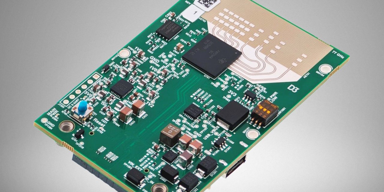
PCB Design Services | Professional PCB Layout & Design - KKPCB
 
HomeCategory

PCB Design Services | Professional PCB Layout & Design - KKPCB

High Layer Count PCB: Advanced Multilayer PCB Design for Complex Electronics

As electronic systems become more powerful and complex, standard multilayer PCBs are sometimes no longer sufficient. Advanced applications such as telecommunications infrastructure, data servers, and aerospace electronics often require extremely dense routing and precise signal control. This is where High Layer Count PCBs come into play. These circuit boards typically contain 20 layers or more,...

Buried Via PCB: Advanced PCB Design for High-Density and High-Speed Electronics

As electronic devices become smaller and more powerful, PCB designers face a constant challenge: fitting more circuitry into less space. Traditional through-hole vias can quickly consume valuable routing area, especially in multilayer boards. This is where Buried Via PCB technology becomes extremely useful. By placing vias entirely within internal layers, designers can maximize routing space...

Probe Card PCB: Design, Materials and Manufacturing for Semiconductor Wafer Testing

Before a semiconductor chip ever reaches packaging, it must first prove itself on the wafer. Engineers run electrical tests directly on the silicon to identify defective dies early in the manufacturing process. This delicate operation relies on a specialized testing interface known as a Probe Card. At the heart of this system lies the Probe...

ATE Test PCB: Design, Materials and Applications in Modern Electronics Testing

In modern electronics manufacturing, accuracy is everything. Before a chip or circuit board reaches the market, it must go through rigorous testing to verify functionality, reliability, and performance. This process is typically carried out using Automated Test Equipment (ATE). At the center of this system lies the ATE Test PCB, a specialized printed circuit board...

Custom ATE PCB: Designing High-Performance Test Boards for Automated Test Equipment

Custom ATE PCB: Designing High-Performance Test Boards for Automated Test Equipment In modern electronics manufacturing, Custom ATE PCB (Automated Test Equipment PCB) plays a crucial role in ensuring product quality, reliability, and performance. A custom ATE PCB is specifically designed for test fixtures or testers that interface with electronic devices under test (DUT). These PCBs...

Multilayer PCB: Advanced Design for High-Density and High-Speed Electronics

Multilayer PCB: Advanced Design for High-Density and High-Speed Electronics With modern electronic devices becoming increasingly compact and high-performance, Multilayer PCB technology is essential for achieving complex circuit routing, improved signal integrity, and efficient power distribution. A multilayer PCB consists of three or more conductive copper layers laminated together with dielectric materials , enabling compact, high-density,...

Microvia PCB: High-Density Interconnect Solutions for Advanced Electronics

Microvia PCB: High-Density Interconnect Solutions for Advanced Electronics As electronic devices become smaller, faster, and more complex, designers face increasing challenges in routing high-density circuits. Microvia PCB technology provides a solution by enabling high-density interconnects (HDI), allowing for compact multilayer designs with superior electrical performance. A Microvia PCB uses extremely small vias, typically less than...

High Current PCB: Design Principles for Reliable Power Delivery

High Current PCB: Design Principles for Reliable Power Delivery Modern electronic devices and industrial systems increasingly require PCBs capable of handling high currents. A High Current PCB is specifically engineered to safely transmit large amounts of electrical current while minimizing heat generation, voltage drop, and reliability risks. These PCBs are widely used in power electronics,...

Power Integrity PCB: Ensuring Stable Power Delivery for High-Speed Electronics

Power Integrity PCB: Ensuring Stable Power Delivery for High-Speed Electronics As modern electronic systems operate at increasingly high speeds, maintaining Power Integrity (PI) on printed circuit boards is critical. Power Integrity PCB design ensures that all components receive clean, stable voltage, minimizing noise, voltage drop, and electromagnetic interference (EMI). Poor power integrity can cause timing...

Fine Line PCB: High-Density Circuit Design for Advanced Electronics

Fine Line PCB: High-Density Circuit Design for Advanced Electronics As electronic devices continue to become smaller, faster, and more integrated, traditional PCB manufacturing technologies are often insufficient to meet the demands of modern circuit density. Fine Line PCB technology enables the creation of extremely narrow traces and spaces, allowing engineers to design highly compact and...