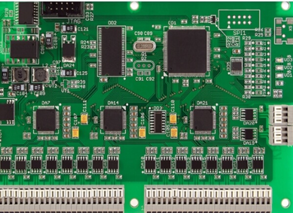
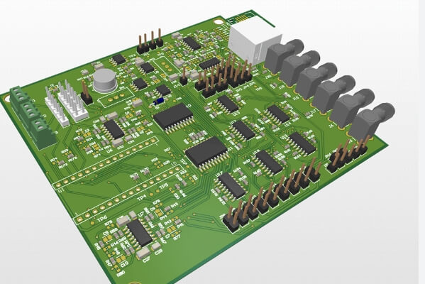
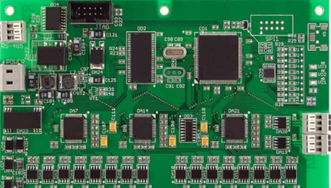
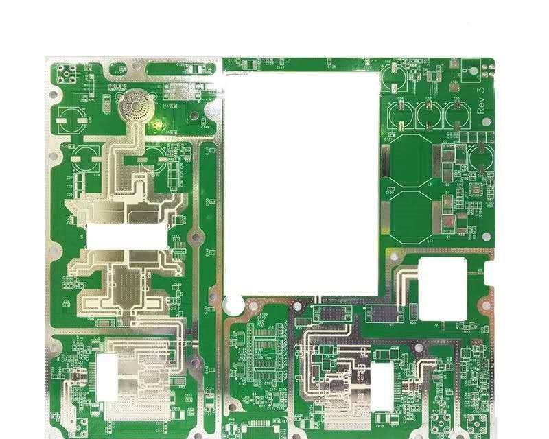
Before explaining the inspection work after PCB wiring is completed, we will first introduce three special PCB routing techniques. The routing of PCB LAYOUT will be explained from three aspects: right-angle routing, differential routing, and serpentine routing: Right-angle routing (three aspects) The impact of right-angle routing on signals is mainly reflected in three aspects: first, the corner...
HomeAuthor
kkpcba-Cindy - KKPCB - Page 44 of 75
Electrostatic Discharge (ESD) can damage sensitive components such as MOSFETs, CMOS gates, and PN junctions, leading to issues like gate damage, short circuits, and even melted wiring. This guide offers practical strategies to design PCBs that effectively prevent ESD from harming the circuit. Key ESD Prevention Techniques for PCB Design 1. Layering Techniques Multi-layer PCBs: Use...
As electronic products become more advanced, they encounter more sources of electromagnetic interference (EMI) that can disrupt device function and potentially harm health. This guide explores strategies for designing PCB boards with optimized electromagnetic compatibility (EMC), focusing on reducing interference and increasing product resilience. 1. PCB Board Design PCB boards are essential components in electronic devices, providing...
Based on recent trends, improving efficiency is a key goal, and the trade-off of using slow switching devices for better EMI is not worth it. Superjunctions can improve efficiency in applications where planar MOSFETs struggle. Superjunction MOSFETs significantly reduce on-resistance and parasitic capacitance compared to traditional planar MOSFET technology. The significant reduction in on-resistance and...
In PCB design, one common question arises: if an extra layer is not required for routing, why use it? Reducing the number of layers theoretically makes the board thinner and lowers costs. However, in some cases, adding an additional layer can actually reduce costs. Core Structures of Multilayer PCBs PCBs have two main structures: core structure and...
Engineering TechnologiesCustomer CaseElectronics Industry NewsPCB DesignPCB ManufacturingPCB Materials
Understand the performance and applications of Rogers 6010 and aluminum based high-frequency PCB
Introduction: Choosing the Right High-Frequency PCB Material In modern high-frequency PCB design, material selection plays a decisive role in determining signal integrity, thermal performance, and overall system reliability. Among the most widely used materials, Rogers 6010 and aluminum-based high-frequency PCB solutions stand out for their unique advantages in RF applications, microwave circuits, and high-power electronic...
When replacing an IC in PCB circuit design, the following tips can help designers make more efficient and effective PCB designs. 1. Direct Replacement Direct replacement involves swapping the original IC with a new one without modifying the design. The replacement IC should match the original IC’s main functions, performance indicators, package form, pin configuration, pin...
With the advancement of policies by the National People’s Congress and the Chinese People’s Political Consultative Conference supporting entrepreneurship and innovation, the electronics industry has been rapidly transforming, propelling us into the intelligent era. In this context, upgrading PCB copy board design technology has become essential. With the expansion of the smartphone and tablet markets,...
RF (Radio Frequency) PCB design is often described as a “black art” because there are still many uncertainties in theory, but this view is only partially correct. There are also many rules and regulations that can be followed in RF PCB design and should not be ignored. However, in actual design, the real practical skill is...
In PCB design, effective ESD (Electrostatic Discharge) protection can be achieved through strategic layering, layout, and installation adjustments. ESD protection aims to shield delicate semiconductor chips from static electricity originating from humans, the environment, or even other electronic components, which can damage insulation layers, MOSFET and CMOS gates, PN junctions, and wiring. Here are some recommended techniques...

