
PCB routing is one of the most important stages in printed circuit board design. A well-designed routing strategy directly affects:
- Signal integrity
- Power integrity
- Electromagnetic compatibility (EMC)
- Thermal performance
- Manufacturing reliability
With the increasing complexity of electronic products, traditional point-to-point routing methods are often insufficient for advanced applications. High-speed digital systems, RF circuits, power electronics, and high-density PCBs require specialized routing techniques to control electrical performance and reduce potential failures.
Among various PCB routing approaches, three special wiring methods are frequently used in advanced PCB design:
- Differential Pair Routing
- Serpentine Routing
- Guard Trace Routing
Each method addresses different design challenges, including noise reduction, timing control, and interference prevention.
1. Differential Pair Routing
1.1 What Is Differential Pair Routing?
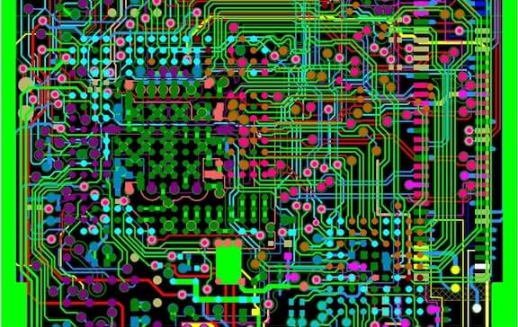
Differential pair routing is a PCB wiring method where two signal traces carry equal-amplitude but opposite-polarity signals.
The receiver detects the voltage difference between the two lines rather than the voltage level of a single signal.
Common differential interfaces include:
- USB
- HDMI
- LVDS
- Ethernet
- PCIe
- High-speed ADC interfaces
A differential pair typically consists of:
- Positive signal line (+)
- Negative signal line (-)
1.2 Advantages of Differential Routing
Improved Noise Immunity
Because external noise tends to couple similarly into both traces, the receiver can reject common-mode interference.
Benefits include:
- Lower EMI sensitivity
- Improved signal stability
- Better performance in noisy environments
Reduced Electromagnetic Radiation
The current flowing in opposite directions creates electromagnetic fields that partially cancel each other.
This helps reduce:
- Radiated emissions
- Crosstalk
- EMC issues
Supports High-Speed Signal Transmission
Differential signaling is widely used in high-speed systems because it provides:
- Better signal integrity
- Lower voltage swing requirements
- Higher transmission speed capability
1.3 Differential Pair PCB Design Guidelines
Maintain Constant Spacing
The distance between the two traces should remain consistent throughout the route.
Avoid:
- Sudden spacing changes
- Unequal geometry
- Excessive separation
Match Trace Length
The two traces should have similar lengths.
Length mismatch can introduce:
- Timing skew
- Signal distortion
Keep Reference Plane Continuous
Differential pairs should preferably be routed above a continuous ground plane.
Avoid:
- Crossing plane gaps
- Changing reference layers unnecessarily
Control Impedance
Common differential impedance values include:
- 90 Ω
- 100 Ω
depending on interface requirements.
Impedance depends on:
- Trace width
- Trace spacing
- Dielectric thickness
- PCB material properties
2. Serpentine Routing
2.1 What Is Serpentine Routing?
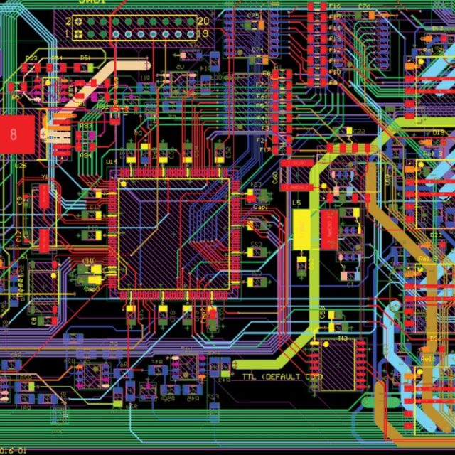
Serpentine routing is a PCB routing technique where a trace is intentionally routed in a zigzag pattern to increase its electrical length within a limited area.
It is mainly used for:
- Signal length matching
- Timing synchronization
Common applications include:
- DDR memory interfaces
- High-speed buses
- Clock synchronization circuits
2.2 Why Is Serpentine Routing Needed?
High-speed digital systems often require multiple signals to arrive at the receiver within a specific timing window.
Different trace lengths create:
- Different propagation delays
- Timing mismatches
- Data sampling errors
Serpentine routing compensates for shorter traces by adding controlled length.
2.3 Design Considerations for Serpentine Routing
Avoid Excessive Length Compensation
Too much meandering may introduce:
- Additional parasitic capacitance
- Increased inductance
- Signal distortion
Length matching should only compensate for necessary differences.
Maintain Proper Spacing
Parallel sections of serpentine traces can couple with each other.
Recommended practices:
- Keep sufficient spacing between adjacent segments.
- Avoid tightly packed zigzag structures.
Use Smooth Bends
Sharp corners can increase impedance discontinuity.
Preferred:
- Rounded corners
- 45-degree bends
Avoid unnecessary right-angle routing.
2.4 Applications of Serpentine Routing
Common applications include:
DDR Memory
Used for:
- Data line matching
- Clock/data synchronization
High-Speed Communication
Used in:
- Ethernet
- PCIe
- High-speed converters
Clock Distribution
Used to:
- Reduce timing differences
- Improve synchronization
3. Guard Trace Routing
3.1 What Is Guard Trace Routing?
Guard trace routing is a technique where a grounded copper trace is placed beside a sensitive signal trace to reduce interference.
The guard trace acts as a shielding structure between:
- Sensitive signals
- Noise sources
It is commonly used for:
- Analog signals
- RF signals
- High-impedance circuits
3.2 Advantages of Guard Traces
Reduces Crosstalk
Guard traces reduce electromagnetic coupling between nearby traces.
They are useful when routing:
- Low-level analog signals
- Sensor signals
- RF lines
near noisy circuits.
Improves Signal Protection
Sensitive signals are protected from:
- Digital switching noise
- Clock interference
- Power supply noise
Enhances EMC Performance
Proper grounding of guard traces helps reduce:
- Radiated interference
- Noise coupling
3.3 Guard Trace Design Guidelines
Connect Guard Traces to Ground
A floating guard trace may become an antenna and increase interference.
Recommended:
- Connect guard traces to a stable ground plane.
- Add ground vias when appropriate.
Add Stitching Vias
For high-frequency applications, grounding vias along the guard trace improve shielding effectiveness.
Typical applications:
- RF PCB design
- Microwave circuits
- Sensitive analog sections
Maintain Appropriate Spacing
The guard trace should not be placed too close to the signal trace.
Insufficient spacing may:
- Increase capacitance
- Affect impedance
4. Comparison of Three Special Wiring Methods
| Routing Method | Main Purpose | Typical Applications |
|---|---|---|
| Differential Pair Routing | Improve high-speed signal integrity and noise immunity | USB, Ethernet, PCIe, LVDS |
| Serpentine Routing | Match signal length and reduce timing skew | DDR, high-speed buses, clocks |
| Guard Trace Routing | Reduce interference and protect sensitive signals | RF, analog, sensor circuits |
5. How to Select the Appropriate Routing Method
For High-Speed Digital Systems
Recommended:
- Differential routing
- Length matching
- Controlled impedance
Examples:
- Communication equipment
- Data processing systems
- AI hardware
For Timing-Sensitive Interfaces
Recommended:
- Serpentine routing
- Delay matching
Examples:
- Memory interfaces
- High-speed processors
For Sensitive Analog and RF Circuits
Recommended:
- Guard traces
- Ground shielding
- Isolation techniques
Examples:
- Sensor systems
- Medical electronics
- RF modules
6. Manufacturing Considerations
Special routing techniques require cooperation between PCB design and manufacturing processes.
Important considerations include:
Controlled Impedance Manufacturing
Requires accurate control of:
- Dielectric thickness
- Copper thickness
- Trace width
PCB Layer Alignment
High-density routing requires:
- Precise registration
- Stable multilayer fabrication
Signal Integrity Verification
Before production, engineers should evaluate:
- Impedance simulation
- Crosstalk analysis
- Timing analysis
DFM Review
A manufacturing review can identify:
- Excessively narrow traces
- Difficult via structures
- Routing density issues
- Assembly risks
Conclusion
Special PCB wiring methods are essential techniques for modern electronic products where signal speed, reliability, and interference control are critical.
The three commonly used methods include:
- Differential pair routing for high-speed and noise-resistant signal transmission
- Serpentine routing for precise timing and length matching
- Guard trace routing for protecting sensitive signals from interference
Selecting the correct routing strategy requires understanding the electrical characteristics of the circuit, system requirements, and manufacturing limitations.
With proper PCB stack-up design, impedance control, grounding strategy, and DFM analysis, these advanced routing methods can significantly improve PCB performance and reliability in applications such as communication equipment, industrial control systems, automotive electronics, and high-speed computing platforms.
