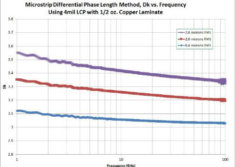
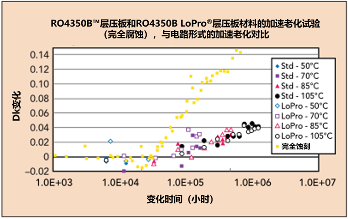
kkpcba-Cindy - KKPCB - Page 42 of 73
 
HomeAuthor

kkpcba-Cindy - KKPCB - Page 42 of 73

Understanding and Improving PCB Open Circuits: Causes and Solutions

Open circuits and short circuits are common issues that PCB manufacturers encounter, often leading to shipment delays, customer complaints, and costly production interruptions. With over 20 years of experience in the PCB manufacturing industry—covering production, quality management, process optimization, and cost control—I have gathered valuable insights into addressing these challenges. Below is a summary of the main causes of PCB...

PCB Drawing: A Summary of Key Practices from Years of Experience

After years of experience in PCB design, certain best practices have emerged. Here, we outline essential aspects of PCB layout, wiring, copper plating, and more, with a focus on optimizing performance and manufacturability. 1. Layout and Wiring Impact on Electrical Performance Separate Digital and Analog Ground: Although challenging, separating these can reduce noise. Understanding IC electrical...

Key Grounding Techniques in Electronic Design

Grounding is fundamental in electronic PCB circuit design, influencing stability, noise immunity, and overall performance. Grounding techniques range from basic single-loop analog grounding to advanced grounding methods for complex mixed-signal designs. These techniques become increasingly critical in high-frequency or high-EMC (Electromagnetic Compatibility) environments. Here’s a comprehensive overview of grounding techniques and methods for reducing ground loops to enhance...

Detailed explanation of three special PCB wiring methods

Before explaining the inspection work after PCB wiring is completed, we will first introduce three special PCB routing techniques. The routing of PCB LAYOUT will be explained from three aspects: right-angle routing, differential routing, and serpentine routing: Right-angle routing (three aspects) The impact of right-angle routing on signals is mainly reflected in three aspects: first, the corner...

Complete Guide to ESD Prevention in PCB Design

Electrostatic Discharge (ESD) can damage sensitive components such as MOSFETs, CMOS gates, and PN junctions, leading to issues like gate damage, short circuits, and even melted wiring. This guide offers practical strategies to design PCBs that effectively prevent ESD from harming the circuit. Key ESD Prevention Techniques for PCB Design 1. Layering Techniques Multi-layer PCBs: Use...

Electromagnetic Compatibility (EMC) Design in PCB Boards

As electronic products become more advanced, they encounter more sources of electromagnetic interference (EMI) that can disrupt device function and potentially harm health. This guide explores strategies for designing PCB boards with optimized electromagnetic compatibility (EMC), focusing on reducing interference and increasing product resilience. 1. PCB Board Design PCB boards are essential components in electronic devices, providing...

How to optimize PCB design to maximize the performance of superjunction MOSFETs

Based on recent trends, improving efficiency is a key goal, and the trade-off of using slow switching devices for better EMI is not worth it. Superjunctions can improve efficiency in applications where planar MOSFETs struggle. Superjunction MOSFETs significantly reduce on-resistance and parasitic capacitance compared to traditional planar MOSFET technology. The significant reduction in on-resistance and...

Balanced PCB Stack-Up Design Method

In PCB design, one common question arises: if an extra layer is not required for routing, why use it? Reducing the number of layers theoretically makes the board thinner and lowers costs. However, in some cases, adding an additional layer can actually reduce costs. Core Structures of Multilayer PCBs PCBs have two main structures: core structure and...

In the ever-evolving landscape of electronics, high-frequency printed circuit boards (PCBs) are crucial for enabling advanced communication technologies. Among the materials dominating this sector, Rogers 6010 and aluminum-based substrates stand out for their unique properties and performance capabilities. This article explores the characteristics, advantages, and applications of these materials, shedding light on their significance in modern electronics....

IC Replacement Skills in PCB Circuit Design

When replacing an IC in PCB circuit design, the following tips can help designers make more efficient and effective PCB designs. 1. Direct Replacement Direct replacement involves swapping the original IC with a new one without modifying the design. The replacement IC should match the original IC’s main functions, performance indicators, package form, pin configuration, pin...