
As electronic products continue to move toward higher integration, faster signal transmission, and smaller form factors, multilayer PCB technology has become essential for modern electronic design. Among various multilayer structures, the 6-layer PCB stackup is one of the most commonly used configurations because it provides a good balance between routing capability, signal integrity, power distribution, manufacturing complexity, and cost.
A properly designed 6-layer PCB can support applications requiring:
- High-speed digital interfaces
- Mixed-signal circuits
- Power management systems
- Industrial control electronics
- Communication equipment
- Automotive electronics
Compared with a 4-layer PCB, a 6-layer board provides additional routing space and improved electromagnetic performance. Compared with higher-layer-count PCBs, it can offer better cost efficiency for medium-complexity designs.
This article explains the structure, advantages, design considerations, and manufacturing aspects of 6-layer PCB stackups.
1. What Is a 6-Layer PCB Stackup?
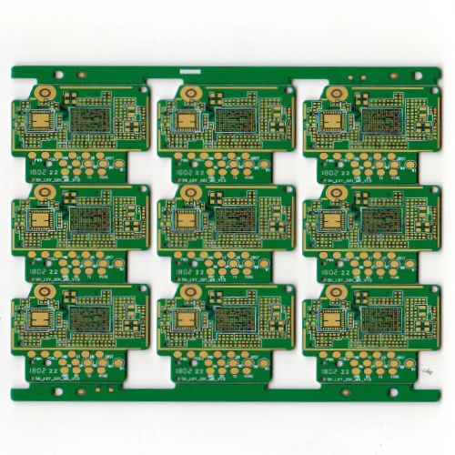
A 6-layer PCB consists of six conductive copper layers separated by insulating dielectric materials.
The layers are typically arranged as:
- Top signal layer
- Internal signal and/or plane layers
- Power and ground planes
- Bottom signal layer
A common 6-layer PCB structure includes:
| Layer | Function |
|---|---|
| Layer 1 | Top signal / Component layer |
| Layer 2 | Ground plane |
| Layer 3 | Internal signal layer |
| Layer 4 | Internal signal layer |
| Layer 5 | Power plane |
| Layer 6 | Bottom signal layer |
This arrangement provides dedicated reference planes for high-speed routing while maintaining efficient layer utilization.
2. Why Choose a 6-Layer PCB?
2.1 More Routing Space
A 6-layer PCB provides additional copper layers compared with 2-layer and 4-layer designs.
Benefits include:
- More signal routing channels
- Easier component escape routing
- Reduced trace congestion
- Better support for complex circuits
This is especially useful for designs containing:
- Multiple ICs
- Fine-pitch components
- High-density connectors
- Large component counts
2.2 Improved Signal Integrity
High-speed signals require stable reference planes to maintain signal quality.
A 6-layer structure allows designers to place signal layers close to:
- Ground planes
- Power planes
This reduces:
- Return path discontinuity
- Electromagnetic radiation
- Crosstalk
Applications involving:
- DDR memory
- Ethernet
- USB
- PCIe
- High-speed ADC interfaces
benefit from optimized 6-layer stackups.
2.3 Better Power Distribution
Dedicated power and ground layers create a low-impedance power distribution network (PDN).
Advantages include:
- Reduced power noise
- Improved voltage stability
- Better transient response
This is important for:
- Microprocessors
- DSP systems
- FPGA boards
- Communication equipment
2.4 Enhanced EMI Performance
A well-designed 6-layer stackup improves electromagnetic compatibility.
Continuous plane layers help:
- Contain electromagnetic fields
- Reduce radiation
- Provide controlled current return paths
This makes 6-layer PCBs suitable for products requiring strict EMC performance.
3. Common 6-Layer PCB Stackup Configurations
Different applications require different stackup arrangements.
3.1 Standard Signal-Power-Ground Stackup
Example:
| Layer | Purpose |
|---|---|
| L1 | Signal |
| L2 | Ground |
| L3 | Signal |
| L4 | Signal |
| L5 | Power |
| L6 | Signal |
Advantages:
- Simple manufacturing
- Good routing flexibility
- Suitable for general industrial electronics
3.2 High-Speed Signal Integrity Stackup
Example:
| Layer | Purpose |
|---|---|
| L1 | High-speed signal |
| L2 | Ground plane |
| L3 | Signal |
| L4 | Power plane |
| L5 | Signal |
| L6 | Ground plane |
Advantages:
- Better return path control
- Reduced EMI
- Improved impedance consistency
Suitable for:
- High-speed processors
- Communication boards
- Data acquisition systems
3.3 Mixed-Signal Stackup
For systems containing both analog and digital circuits:
| Layer | Purpose |
|---|---|
| L1 | Components and signals |
| L2 | Analog/digital ground reference |
| L3 | Digital signals |
| L4 | Power distribution |
| L5 | Analog signals |
| L6 | Signals |
Design focus:
- Noise isolation
- Ground strategy
- Analog signal protection
4. Key Design Considerations for 6-Layer PCBs
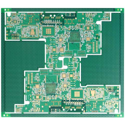
4.1 Layer Assignment Planning
Before routing begins, engineers should define:
- Signal layer allocation
- Power distribution
- Ground reference planes
- High-speed routing requirements
Poor layer planning may result in:
- Difficult routing
- Increased EMI
- Signal integrity problems
4.2 Controlled Impedance Design
High-speed 6-layer PCBs often require controlled impedance.
Important parameters include:
- Trace width
- Copper thickness
- Dielectric thickness
- Material properties
Common impedance requirements include:
- 50 Ω single-ended signals
- 90 Ω differential signals
- 100 Ω differential signals
The PCB stackup should be finalized together with the PCB manufacturer to ensure fabrication accuracy.
4.3 Ground Plane Design
A continuous ground plane is essential for high-performance designs.
Benefits include:
- Lower return path impedance
- Reduced noise coupling
- Improved EMI performance
Avoid:
- Splitting ground planes unnecessarily
- Routing high-speed signals across plane gaps
4.4 Power Plane Optimization
Power layers should be designed considering:
- Current requirements
- Voltage domains
- Noise sensitivity
For complex systems, multiple power rails may require:
- Separate power regions
- Filtering components
- Proper return paths
4.5 High-Speed Signal Routing
For high-speed interfaces, consider:
Differential Pair Routing
Maintain:
- Constant spacing
- Matched lengths
- Controlled impedance
Length Matching
Required for:
- DDR interfaces
- High-speed buses
- Clock/data synchronization
Via Optimization
Vias introduce:
- Inductance
- Capacitance
- Impedance discontinuities
Minimize unnecessary layer transitions.
5. Material Selection for 6-Layer PCBs
Material selection depends on application requirements.
Standard FR-4
Suitable for:
- Industrial control boards
- General electronics
- Low-to-medium speed applications
Advantages:
- Cost-effective
- Widely available
High-Tg FR-4
Suitable for:
- High-temperature environments
- Automotive electronics
- Industrial applications
Advantages:
- Better thermal reliability
- Improved dimensional stability
Low-Loss Materials
For high-frequency applications:
- RF communication
- Microwave circuits
- High-speed networking
materials such as low-loss laminates may be required.
Important parameters include:
- Low dielectric loss (Df)
- Stable dielectric constant (Dk)
- Low signal attenuation
6. Manufacturing Considerations
A successful 6-layer PCB design must consider manufacturing capability.
6.1 Lamination Process
Multilayer PCB manufacturing requires precise lamination control.
Important factors:
- Layer alignment
- Resin flow
- Pressing parameters
Poor control may cause:
- Layer misregistration
- Warpage
- Reliability issues
6.2 Copper Thickness
Copper thickness affects:
- Current carrying capability
- Signal performance
- Manufacturing difficulty
Common copper options include:
- 1 oz copper
- 2 oz copper
- Heavy copper structures for power applications
6.3 Via Structures
6-layer boards may use:
- Through vias
- Blind vias
- Buried vias
- HDI microvias
The choice depends on:
- Density requirements
- Cost considerations
- Component pitch
6.4 PCB Testing
Quality verification may include:
- Electrical testing
- Impedance testing
- AOI inspection
- X-ray inspection (for advanced assemblies)
These processes help ensure manufacturing consistency.
7. Applications of 6-Layer PCBs
Industrial Control Systems
Used in:
- PLC controllers
- Automation equipment
- Motor control systems
Requirements:
- Reliability
- Noise resistance
Communication Equipment
Used in:
- Network devices
- Wireless systems
- Data transmission equipment
Requirements:
- Signal integrity
- Controlled impedance
Automotive Electronics
Used in:
- Vehicle control units
- Battery management systems
- Sensor modules
Requirements:
- Thermal stability
- Long-term reliability
Medical Electronics
Used in:
- Monitoring devices
- Diagnostic equipment
Requirements:
- Low noise
- High reliability
8. DFM Considerations for 6-Layer PCB Design
Early Design for Manufacturability (DFM) analysis helps reduce production risks.
Important review points include:
- Minimum trace width and spacing
- Via size and aspect ratio
- Component placement
- Assembly requirements
- Impedance control feasibility
- Testing accessibility
Close communication between PCB designers and manufacturers improves:
- First-pass yield
- Production efficiency
- Product reliability
Conclusion
A 6-layer PCB stackup provides an effective solution for medium-to-high complexity electronic systems by balancing routing flexibility, signal integrity, power distribution, and manufacturing cost.
Successful 6-layer PCB design requires careful consideration of:
- Layer arrangement
- Impedance control
- Grounding strategy
- Power integrity
- Material selection
- Manufacturing capability
With proper stackup planning and DFM evaluation, 6-layer PCBs can support advanced applications including industrial automation, communication equipment, automotive electronics, and high-speed digital systems while maintaining reliable electrical performance and production stability.
