
Introduction
In high-frequency and microwave PCB manufacturing, every material choice can directly influence electrical performance.
While laminate selection is often considered the primary factor affecting RF performance, copper foil characteristics also play a critical role in determining:
- signal loss
- impedance stability
- phase consistency
- insertion loss
- long-term reliability
For applications such as:
- 5G communication equipment
- automotive radar systems
- satellite communication
- aerospace electronics
- high-speed computing platforms
- microwave modules
the selection of suitable copper foil becomes an essential part of PCB engineering design.
At KKPCB, we evaluate copper foil properties together with laminate materials, stack-up structures, and transmission line requirements to achieve stable high-frequency PCB performance.
Understanding Copper Foil in High-Frequency PCB Manufacturing
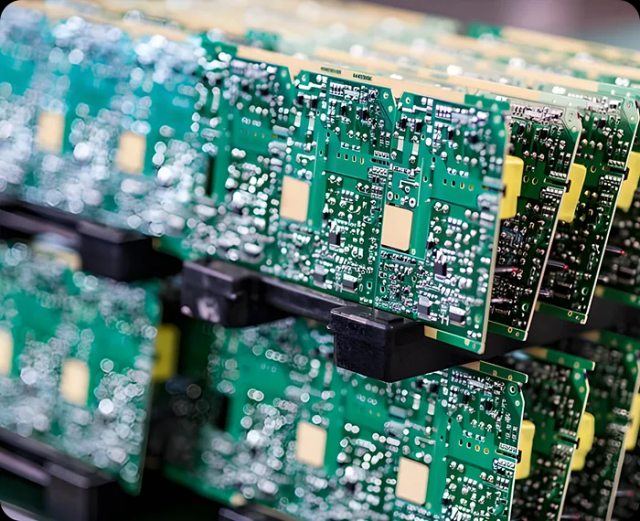
Copper foil serves as the conductive layer of a printed circuit board, forming the transmission paths that carry electrical signals.
Unlike conventional low-frequency PCB applications, high-frequency circuits are more sensitive to copper surface characteristics because RF signals travel mainly along the conductor surface due to the skin effect.
At higher frequencies:
- current distribution becomes concentrated near the copper surface;
- surface roughness increases conductor loss;
- uneven copper profiles may affect impedance and phase stability.
Therefore, copper foil selection is not only a manufacturing consideration but also an important RF design parameter.
Main Types of Copper Foil Used in PCB Fabrication
Copper foils used in high-frequency PCB manufacturing are mainly classified into:
1. Electrodeposited Copper Foil (ED Copper)
Electrodeposited copper foil is produced through an electrochemical deposition process.
During manufacturing:
- Copper ions are deposited onto a rotating titanium drum.
- Copper gradually forms into a continuous foil layer.
- Surface treatments are applied to improve adhesion with dielectric materials.
Characteristics of ED Copper
Advantages:
- higher tensile strength
- good mechanical reliability
- widely compatible with PCB manufacturing processes
- suitable for standard multilayer PCB applications
However, traditional ED copper usually has a rougher surface profile, which may increase:
- conductor loss
- insertion loss
- signal attenuation
at high frequencies.
2. Rolled Copper Foil (RA Copper)
Rolled copper foil is manufactured through mechanical rolling processes that reduce copper thickness while extending its length.
Compared with ED copper, rolled copper has:
- smoother surface morphology
- better flexibility
- improved resistance against cracking during bending
Advantages of Rolled Copper
Rolled copper is commonly selected for:
- flexible PCBs
- rigid-flex PCBs
- high-frequency RF circuits
- applications requiring low conductor loss
Its smoother surface helps reduce RF signal degradation, especially in microwave and millimeter-wave designs.
Copper Roughness and Its Impact on RF Signal Performance
Copper surface roughness is a critical factor affecting high-frequency signal transmission.
When copper surfaces are rough:
- RF current travels through a longer conductive path;
- effective conductor resistance increases;
- insertion loss becomes higher.
Research on microwave transmission lines shows that copper roughness can significantly influence conductor loss, especially at frequencies above several GHz.
For example:
A smoother copper foil can provide:
- lower insertion loss
- better phase stability
- improved signal consistency
while rougher copper surfaces may cause:
- increased attenuation
- impedance variation
- reduced transmission efficiency
This becomes increasingly important for:
- 77 GHz automotive radar
- mmWave communication systems
- high-speed data transmission boards
Copper Foil Roughness and Effective Dielectric Constant
Copper surface profile can also influence the effective dielectric constant of transmission lines.
Higher copper roughness may cause:
- longer electromagnetic propagation paths;
- changes in phase velocity;
- deviation from expected impedance values.
For high-speed and RF PCB designs, even small variations can impact:
- timing accuracy
- phase matching
- antenna performance
Therefore, copper roughness should be considered during:
Low-Profile Copper Foil Technology
To balance adhesion and electrical performance, advanced copper foil technologies have been developed.
Reverse Treated Copper Foil (RTF)
Reverse treated copper applies surface treatment on the smooth side of ED copper.
Benefits include:
- improved dielectric bonding
- reduced conductor roughness
- better high-frequency performance
Low Profile (LP) Copper Foil
Low-profile copper minimizes surface roughness while maintaining sufficient bonding strength.
Advantages:
- reduced insertion loss
- improved signal integrity
- suitable for high-speed PCB applications
Common applications include:
- 5G communication boards
- high-frequency modules
- advanced networking equipment
Mechanical Reliability Considerations
Copper foil selection also affects PCB mechanical performance.
Thermal Shock Resistance
During thermal cycling:
- ED copper may experience stress concentration in narrow traces;
- rolled copper provides better flexibility and crack resistance.
This makes rolled copper advantageous for:
- flexible circuits
- repeated bending applications
- harsh environmental conditions
Copper Adhesion Performance
Copper foil must maintain strong adhesion with dielectric materials.
Surface treatment improves:
- peel strength
- lamination reliability
- resistance against delamination
However, for high-frequency materials such as PTFE-based laminates, excessive copper roughness may negatively affect electrical performance.
Therefore, manufacturers must balance:
adhesion reliability vs RF performance
Comparison Between ED Copper and Rolled Copper
| Property | ED Copper | Rolled Copper |
|---|---|---|
| Manufacturing Method | Electrochemical deposition | Mechanical rolling |
| Surface Roughness | Higher | Lower |
| RF Loss Performance | Moderate | Excellent |
| Flexibility | Lower | Higher |
| Thermal Cycling Resistance | Good | Excellent |
| High-Frequency Application | General RF | Advanced RF/mmWave |
| Manufacturing Cost | Lower | Higher |
Copper Foil Selection for Different PCB Applications
High-Speed Digital PCB
Recommended considerations:
- low-profile copper
- controlled roughness
- stable impedance performance
Applications:
- servers
- switches
- high-speed computing platforms
RF and Microwave PCB
Important requirements:
- ultra-low copper roughness
- stable phase performance
- low conductor loss
Applications:
- radar systems
- communication modules
- satellite electronics
Flexible and Rigid-Flex PCB
Preferred material:
- rolled copper foil
Because of:
- excellent bending durability
- reduced copper fatigue
- mechanical reliability
KKPCB Engineering Approach for Copper Foil Selection
At KKPCB, copper foil selection is integrated into the complete PCB engineering process.
Our engineers consider:
Material Compatibility
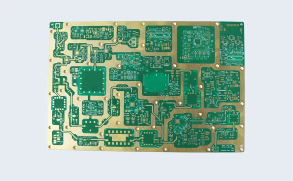
Matching copper foil with:
- Rogers RO3003
- RO4003C
- RO4350B
- RT/duroid materials
- PTFE-based laminates
RF Performance Optimization
Including:
- impedance control
- insertion loss evaluation
- transmission line optimization
- stack-up simulation
Manufacturing Reliability
Through:
- controlled lamination processes
- copper thickness verification
- surface treatment control
- AOI inspection
- electrical testing
Conclusion
Copper foil is more than a conductive layer in high-frequency PCB manufacturing.
Its:
- surface roughness
- manufacturing method
- mechanical properties
- bonding characteristics
directly influence PCB electrical performance and reliability.
For advanced applications such as RF communication, automotive radar, aerospace electronics, and high-speed systems, selecting the appropriate copper foil technology is essential for achieving:
- lower signal loss
- stable impedance
- improved reliability
- consistent production performance
With experience in high-frequency PCB fabrication and advanced laminate processing, KKPCB supports customers in selecting optimized material solutions for demanding electronic applications.
