kkpcba-Cindy - KKPCB - Page 14 of 66
 
HomeAuthor

kkpcba-Cindy - KKPCB - Page 14 of 66

Advantages and applications of single-sided PCB

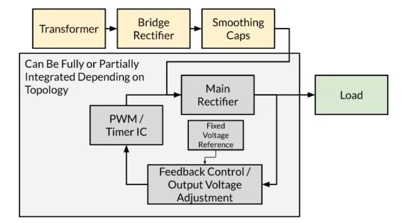
What is a Single-Sided PCB? A Single-Sided PCB (also known as a Single-Layer PCB or One-Layer PCB) is the simplest and most cost-effective type of printed circuit board. As the name suggests, it has a single conductive layer (usually copper) on one side of the substrate, with the electronic components mounted on the opposite side. Unlike double-sided PCBs, which feature conductive layers on both sides, single-sided...

Multilayer PCB Manufacturing Process, Advantages and Applications

1. Introduction: Why Multilayer PCBs Are Essential in Modern Electronics As electronic devices continue to evolve toward miniaturization, high-speed performance, and multifunction integration, traditional single-layer or double-layer PCBs can no longer meet design requirements. This has led to the widespread adoption of multilayer PCBs (Multilayer Printed Circuit Boards), which integrate multiple conductive layers within a...

PCB Layout Planning – Packages and Routing

PCB layout planning is a critical phase in the design process, enabling engineers to save time and ensure a structured approach to package management, component placement, and routing. Proper planning ensures that the design meets electrical, spacing, and physical requirements before moving to the actual layout stage. This article explores key aspects of PCB layout planning, focusing on footprint management, routing strategies,...

How to Create a Variable Power Supply PCB Layout

A variable power supply allows the user to vary and adjust the desired output voltage and current. This type of power supply circuit includes an adjustable voltage regulator that can be set according to a specified input. An adjustable voltage regulator features both line regulation and load regulation. Unlike fixed power supplies that provide a...

Advanced PCB Footprint Generator: Key to Efficient PCB Design

Why PCB Footprint Accuracy Matters In modern high-speed PCB design, HDI PCB development, and high-density electronic systems, the accuracy of PCB footprints (land patterns) directly impacts: Assembly yield Solder joint reliability Manufacturing efficiency Time-to-market A poorly designed footprint can result in: Component misalignment Solder bridging or tombstoning Rework and production delays This is why advanced...

Optimizing PCB Trace Thickness vs. Current Capacity

The relationship between PCB trace thickness and current capacity is a critical aspect of PCB design. Properly sizing traces ensures that they can handle the required current without overheating, which is essential for the reliability and functionality of the circuit. This article explores the key considerations for selecting trace thickness, the impact of copper weight, and...

PCB Resistors and Board Design

PCB resistors are designed to be mounted and soldered to printed circuit boards; they control current flow and divide voltages, among other things.  PCB resistors come in many shapes and sizes, but they’re all designed to fit easily into board layouts. They have two terminals that can be soldered to the conductive traces on the PCB so they...

KKPCB Case Study: High-Performance Communication Backplane PCB Solution

Introduction: Enabling High-Speed Communication Systems In today’s data-driven world, high-speed communication systems demand exceptional signal integrity, power stability, and system reliability. At the core of these systems lies the communication backplane PCB, which serves as the backbone for high-speed data transmission between multiple modules. This case study highlights how KKPCB delivered a high-performance backplane PCB...

Smart Sensor PCBA Solution Case Study for Industrial Automation

1. Background Overview A European client specializing in industrial automation required a compact, highly reliable smart sensor capable of accurately detecting humidity, temperature, and motion in challenging environments. To meet strict industrial requirements—such as signal integrity, durability, and fast time-to-market—they collaborated with KKPCB to develop a tailored PCBA solution. 2. Application Scenario The smart sensor...